


TMP92CZ26A
92CZ26A-511
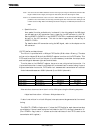
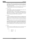
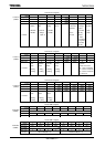
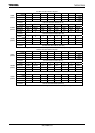
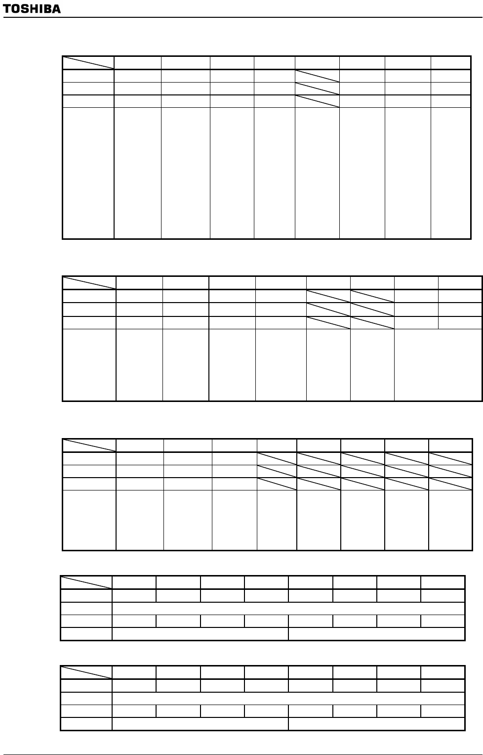
LCD Control 0 Register
7 6 5 4 3 2 1 0
bit Symbol PIPE ALL0 FRMON
–
DLS LCP0OC START
Read/Write R/W R/W R/W R/W R/W R/W R/W
After reset 0 0 0 0 0 0 0
Function
PIP
function
0:Disable
1:Enable
Segment
data
0: Normal
1: Always
output “0”
FR divide
setting
0: Disable
1: Enable
Always
write “0”
FR signal
LCP0/Line
selection
0:Line
1:LCP0
LCP0(Note
0: Always
output
1: At valid
d
ata only
LLOAD
width
0: At setting
in register
1: At valid
d
ata onl
y
LCDC
operation
0: Stop
1: Start
Note: When select STN mode, LCP0 is output at valid data only regardless of the setting of <LCP0OC> bit.
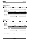
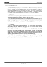
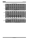
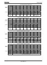
LCD Control 1 Register
7 6 5 4 3 2 1 0
bit Symbol LCP0P LHSP LVSP LLDP LVSW1 LVSW0
Read/Write R/W R/W R/W R/W R/W R/W
After reset 1 0 1 0 0 0
Function
LCP0
phase
0: Rising
1: Falling
LHSYNC
phase
0: Rising
1: Falling
LVSYNC
phase
0: Rising
1: Falling
LLOAD
phase
0: Rising
1: Falling
LVSYNC
enable time control
00: 1 clock of LHSYNC
01: 2 clocks of LHSYNC
10: 3 clocks of LHSYNC
11: Reserved
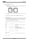
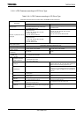
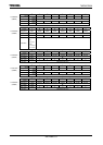
LCD Control 2 Register
7 6 5 4 3 2 1 0
bit Symbol LGOE2P LGOE1P LGOE0P
Read/Write R/W R/W R/W
After reset 0 0 0
Function
LGOE2
phase
0: Rising
1: Falling
LGOE1
phase
0: Rising
1: Falling
LGOE0
phase
0: Rising
1: Falling
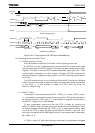
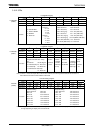
Divide FRM 0 Register
7 6 5 4 3 2 1 0
bit Symbol FMP3 FMP2 FMP1 FMP0 FML3 FML2 FML1 FML0
Read/Write R/W
After reset 0 0 0 0 0 0 0 0
Function LCP0 DVM (bits 3-0) LHSYNC DVM (bits 3-0)
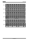
Divide FRM 1 Register
7 6 5 4 3 2 1 0
bit Symbol FMP7 FMP6 FMP5 FMP4 FML7 FML6 FML5 FML4
Read/Write R/W
After reset 0 0 0 0 0 0 0 0
Function LCP0 DVM (bits 7-4) LHSYNC DVM (bit 7-4)
LCDDVM0
(
0283H
)
LCDCTL1
(
0286H
)
LCDCTL2
(0287H)
LCDCTL0
(
0285H
)
LCDDVM1
(
0288H
)