


TMP92CZ26A
92CZ26A-251
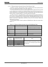
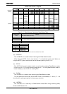
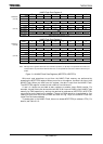
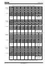
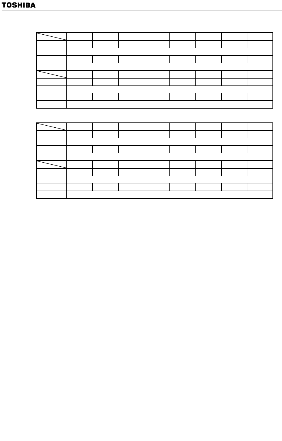
NAND Flash Data Register 0
7 6 5 4 3 2 1 0
bit Symbol D7 D6 D5 D4 D3 D2 D1 D0
Read/Write R/W
After reset Undefined Undefined Undefined Undefined Undefined Undefined Undefined Undefined
Function NAND Flash Data Register (7-0)
15 14 13 12 11 10 9 8
bit Symbol D15 D14 D13 D12 D11 D10 D9 D8
Read/Write R/W
After reset Undefined Undefined Undefined Undefined Undefined Undefined Undefined Undefined
Function NAND Flash Data Register (15-8)
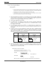
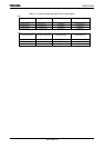
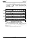
NAND Flash Data Register 1
7 6 5 4 3 2 1 0
bit Symbol D7 D6 D5 D4 D3 D2 D1 D0
Read/Write R/W
After reset Undefined Undefined Undefined Undefined Undefined Undefined Undefined Undefined
Function NAND Flash Data Register (7-0)
15 14 13 12 11 10 9 8
bit Symbol D15 D14 D13 D12 D11 D10 D9 D8
Read/Write R/W
After reset Undefined Undefined Undefined Undefined Undefined Undefined Undefined Undefined
Function NAND Flash Data Register (15-8)
Note: Although these registers allow both read and write operations, no flip-flop is incorporated. Since write and
read operations are performed in different manners, it is not possible to read out the data that has been just
written.
Figure 3.11.6 NAND Flash Data Registers (NDFDTR0, NDFDTR1)
Write and read operations to and from the NAND Flash memory are performed by
accessing the NDFDTR0 register. When you write to this register, the data is written to the
NAND Flash. When you read from this register, the data is read from the NAND Flash.
The NDFDTR0 register is used for both channel 0 and channel 1.
A total of 4 bytes are provided as data registers to enable 4-byte DMA transfer. For
example, 4 bytes of data can be transferred from 32-bit internal RAM to 8-bit NAND Flash
memory by DMA operation by setting the destination address as NDFDTR0. (NDFDTR1
cannot be set as the destination address.) The actual DMA operation is performed by first
reading 4 bytes from the internal RAM and then writing 1 byte to the NAND Flash four
times from the lowest address.
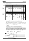
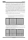
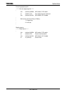
To access data in the NAND Flash, be sure to access NDFDTR0 (at address 1FF0). For
details, see
Table 3.11.3.
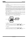
NDFDTR0
(1FF0H)
(1FF1H)
NDFDTR1
(1FF2H)
(1FF3H)