


TMP92CZ26A
92CZ26A-8
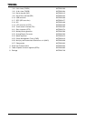
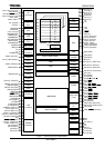
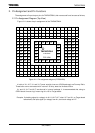
2.2 Pin names and Functions
The names of the input/output pins and their functions are described below.
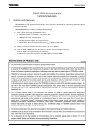
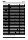
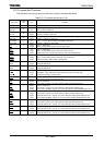
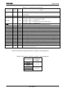
Table 2.2.1 Pin names and functions (1/6)
Pin name
Number of
Pins
I/O Functions
D0 to D7 8 I/O Data: Data bus D0 to D7.
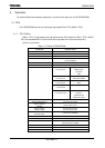
P10 to P17
D8 to D15
8
I/O
I/O
Port 1: I/O port. Input or output is specifiable in units of bit.
Data : Data bus D8 to D15.
P40 to P47
A0 to A7
8
Output
Output
Port 4: Output port.
Address : Address bus A0 to A7.
P50 to P57
A8 to A15
8
Output
Output
Port 5: Output port.
Address : Address bus A8 to A15.
P60 to P67
A16 to A23
8
I/O
Output
Port 6 : I/O port. Input or output is specifiable in units of bit.
Address : Address bus A16 to A23.
P70
RD
1 Output
Output
Port 70 : Output port.
Read : Outputs strobe signal to read external memory.
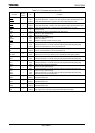
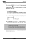
P71
WRLL
NDRE
1 I/O
Output
Output
Port 71 : Output port.
Write : Outputs strobe signal to write data on pins D0 to D7.
NAND Flash read : Outputs strobe signal to read external NAND-Flash.
P72
WRLU
NDWE
1 I/O
Output
Output
Port 72 : I/O port.
Write : Outputs strobe signal to write data on pins D8 to D15.
NAND Flash write : Write enable for NAND Flash.
P73
EA24
1 I/O
Output
Port 73 : I/O port.
Expanded address 24.
P74
EA25
1 I/O
Output
Port 74 : I/O port.
Expanded address 25.
P75
R/
W
NDR/
B
1 I/O
Output
Input
Port 75 : I/O port.
Read/Write : “High” represents read or dummy cycle and “Low” write cycle.
NAND Flash Ready(1) / Busy(0) input.
P76
WAIT
1
I/O
Input
Port 76: I/O port.
Wait: Signal used to request CPU bus wait.
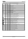
P80
0CS
1
Output
Output
Port 80: Output port.
Chip select 0: Outputs “Low” when address is within specified address area.
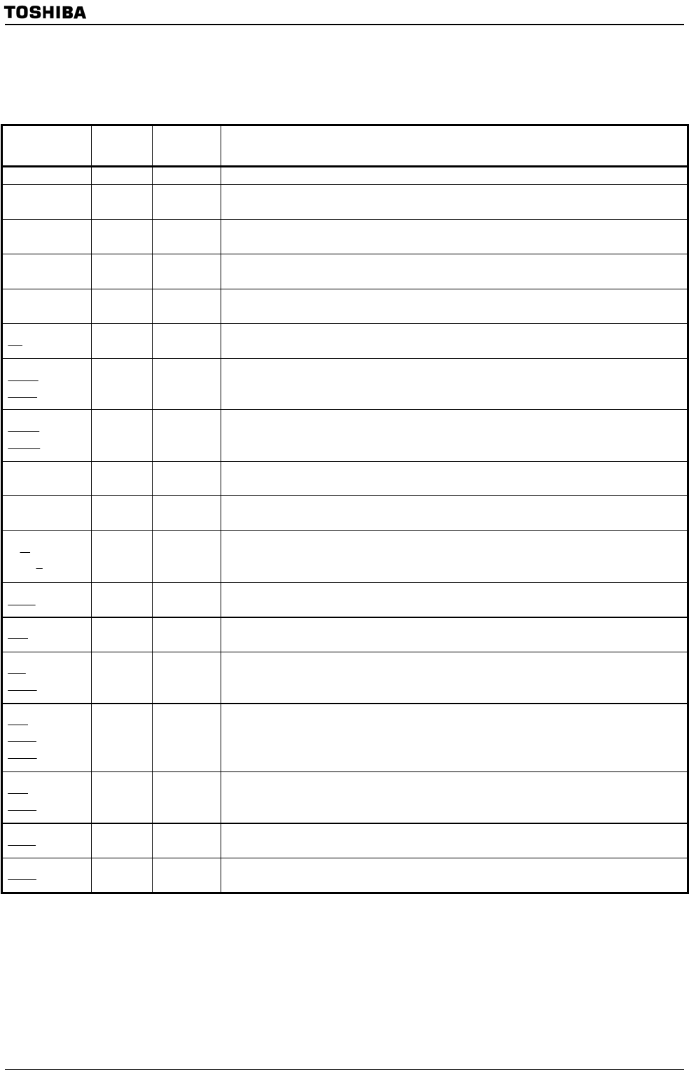
P81
1CS
SDCS
1 Output
Output
Output
Port 81 : Output port
Chip select 1: Outputs “Low” when address is within specified address area.
Chip select for SDRAM : Outputs “Low” when the address is within SDRAM address area.
P82
2CS
CSZA
SDCS
1 Output
Output
Output
Output
Port 82 : Output port.
Chip select 2: Outputs “Low” when address is within specified address area.
Expanded address ZA : Outputs “Low” when address is within specified address area.
Chip select for SDRAM : Outputs “0” when the address is within SDRAM address area.
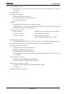
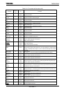
P83
3CS
CSXA
1 Output
Output
Output
Port 83 : Output port.
Chip select 3: Outputs “Low” when address is within specified address area.
Expanded address XA : Outputs “Low” when address is within specified address area.
P84
CSZB
1 Output
Output
Port 84 : Output port.
Expanded address ZB : Outputs “Low” when address is within specified address area.
P85
CSZC
1 Output
Output
Port 85 : Output port.
Expanded address ZC : Outputs “Low” when address is within specified address area.