


TMP92CZ26A
92CZ26A-288
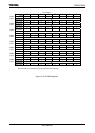
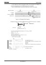
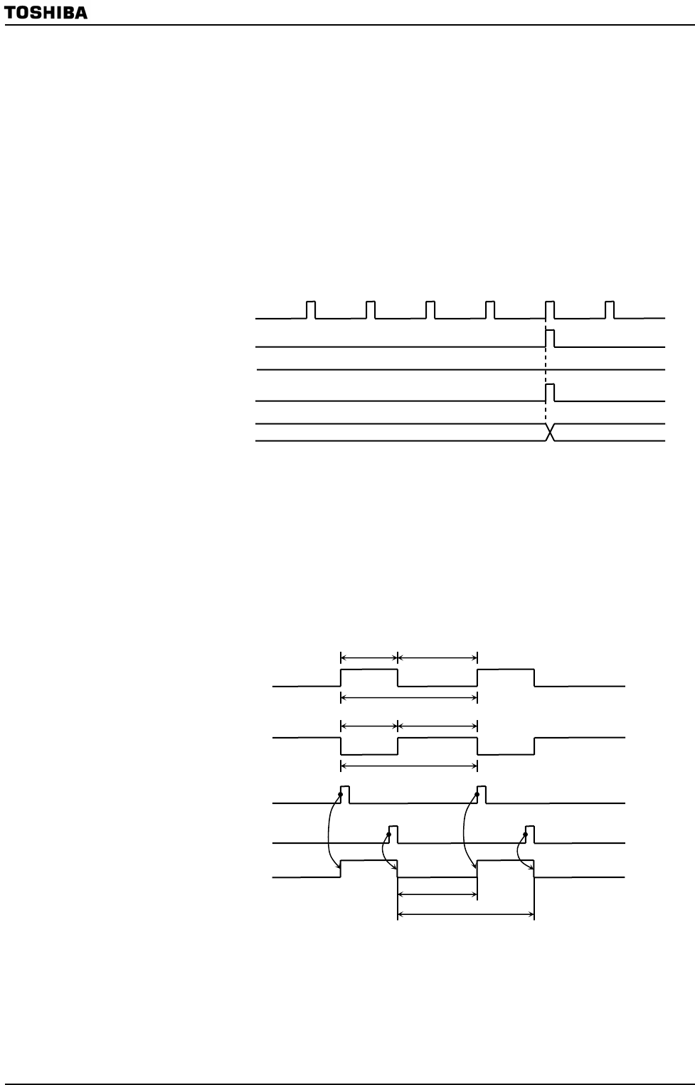
The comparator match signal is output from TMRA0 each time the up counter UC0
matches TA0REG, though the up counter UC0 is not be cleared.
In the case of the TMRA1 comparator, the match detect signal is output on each
comparator pulse on which the values in the up counter UC1 and TA1REG match.
When the match detect signal is output simultaneously from both the comparator
TMRA0 and TMRA1, the up counters UC0 and UC1 are cleared to 0 and the interrupt
INTTA1 is generated. Also, if inversion is enabled, the value of the timer flip-flop
TA1FF is inverted.
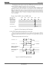
Example: When TA1REG = 04H and TA0REG = 80H
Figure 3.12.19 Timer Output by 16-Bit Timer Mode
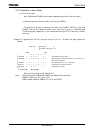
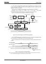
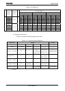
(3) 8-bit PPG (Programmable pulse generation) output mode
Square wave pulses can be generated at any frequency and duty ratio by TMRA0.
The output pulses may be active-low or active-high. In this mode TMRA1 cannot be
used.
TMRA0 outputs pulses on the TA1OUT pin.
Figure 3.12.20 8-Bit PPG Output Waveforms
Inversion
Value of up counte
r
(UC1, UC0)
TMRA0 comparator
match detect signal
Interru
p
t INTTA1
0080H 0180H 0280H 0380H 0480H
Timer out
p
ut TA1OUT
TMRA1 comparator
match detect signal
Interru
p
t INTTA0
0080H
t
TA0REG
TA1REG
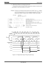
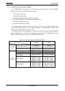
Example: <TA1FFC1:0> = “01”
TA0REG and UC0 match
(Interrupt INTTA0)
TA1REG and UC0 match
(
Interru
p
t INTTA1
)
TA1OUT
t
H
t
L
<TA1FFC1:0> = “10”
t
t
L
t
H
<TA1FFC1:0> = “01”