TMP92CZ26A
92CZ26A-145
3.7.12 Port J (PJ0 to PJ7)
PJ0 to PJ4 and PJ7 are 6-bit output port. Resetting sets the output latch PJ to “1”, and
they output “1”. PJ5 to PJ6 are 2-bit input/output port. In addition to functioning as port,
Port J also functions as output pins for SDRAM (
SDRAS
,
SDCAS
,
SDWE
, SDLLDQM,
SDLUDQM, and SDCKE), SRAM (
SRWR
,
SRLLB
and
SRLUB
) and NAND-Flash(NDALE
and NDCLE). Above setting is used the function register PJFC.
But Output signal either SDRAM or SRAM for PJ0 to PJ2 are selected automatically
according to the setting of memory controller.
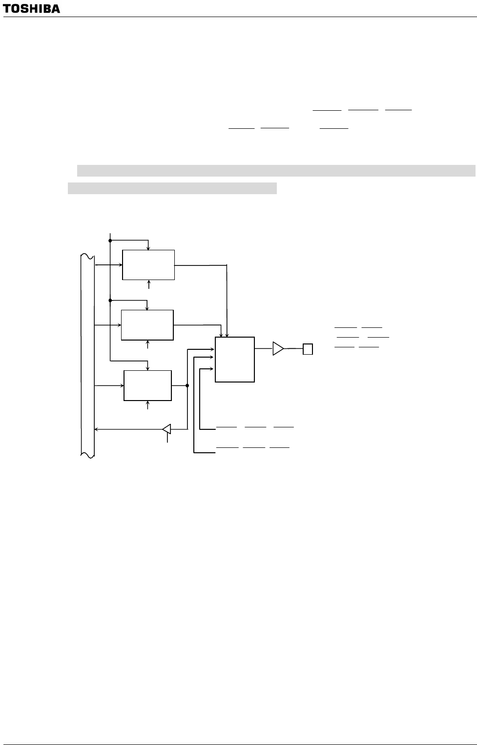
Figure 3.7.31 Port J0 to J4 and J7
S
Function
control
(on bit basis)
Selector
PJ read
Reset
PJ0(
SDRAS
,
SRLLB
)
PJ1 (
SDCAS
,
SRLUB
)
PJ2(
SDWE
,
SRWR
)
PJ3(SDLLDQM)
PJ4(SDLUDQM)
PJ7(SDCKE)
SDRAS
,
SDCAS
,
SDWE
, SDLLDQM, SDLUDQM, SDCKE
Selector
PJFC write
PJ write
Function
control2
(on bit basis)
PJFC2 write
SRLLB
,
SRLUB
,
SRWR
Internal data bus


