Mandatory PCI Configuration Registers — Intel
®
82575EB Gigabit Ethernet Controller
324632-003 Intel
®
82575EB Gigabit Ethernet Controller
Revision: 2.1 Software Developer’s Manual and EEPROM Guide
January 2011 193
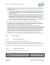
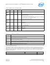
All base registers have the following fields:
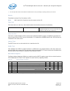
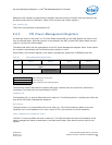
Expansion ROM Base Address
This register is used to define the address and size information for boot-time access to the optional
Flash memory. Only the LAN 0/LAN 1functions can use this window. It is enabled by EEPROM words 24h
and 14h for LAN 0 and LAN 1, respectively. This register returns a zero value for functions without
expansion ROM window.
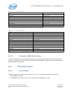
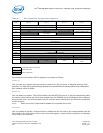
Field Bit(s) RD/WR
Initial
Value
Description
I/O
Address
Space
31:5 R/W 0b These are read/write bits that indicate I/O Bar locations.
Memory
Address
Space
31:4 R/W 0b These are read/write bits hardwired to 0b depending on the memory
mapping window sizes.
• LAN memory spaces are 128K bytes.
• LAN Flash spaces can be 64 KB and up to 8 MB in powers of 2. Mapping
window size is set by the EEPROM word 0Fh.
• MSI-X memory space is 16 KB.
I/O
Address
Space
4:3 RO 0b Hardwired to 0b to indicate an I/O space of 32 bytes.
Prefetch
Memory
3 R 0b The 82575 implements non-prefetchable space due to side effects of read
transactions.
0b = Non-prefetchable space
1b = Prefetchable space
Memory
Type
2:1 R 32-bit =
00b
This field indicates the address space size.
00b = 32-bit
Memory 0 R Memory
= 0b
I/O = 1b
If this bit equals 0b, it indicates memory space. If it equals 1b, it indicates
input/output.
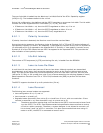
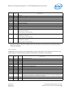
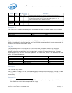
Table 63. Memory & I/O Mapping
Mapping
Window
Mapping Description
Memory
BAR 0
The internal registers and memories are accessed as direct memory mapped offsets from the base address
register. Software accesses can be Dword or 64 bytes.
Flash
BAR 1
The external Flash can be accessed using direct memory mapped offsets from the Flash BAR. Software accesses
can be byte, word, Dword or 64 bytes.
I/O
BAR 2
All internal registers, memories, and Flash can be accessed using I/O operations. There are two 4-byte registers
in the I/O mapping window: Address Register and Data Register. Software accesses can be byte, word or Dword.
MSI-X Bar 3 The internal registers and memories are accessed as direct memory mapped offsets from the Base Address
register. Software accesses can be Dword or 64 bytes.
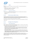
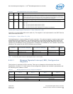
Bits 31:11 Bits 10:1 Bit 0
Expansion ROM BAR (R/W - 31:12316; ‘0’ - 22/15:1) En


