Intel
®
82575EB Gigabit Ethernet Controller — Power Management Interconnects
Intel
®
82575EB Gigabit Ethernet Controller 324632-003
Software Developer’s Manual and EEPROM Guide Revision: 2.1
218 January 2011
82575 support for Active State Link Power Management is reported via the PCIe* Active State Link PM
Support register loaded from the EEPROM.
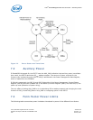
While in L0 state, the 82575 transitions the transmit lane(s) into L0s state once the idle conditions are
met for a period of time as shown in Figure 24.
L0s configuration fields are:
• L0s enable - The default value of the Active State Link PM Control field in the PCIe* Link Control
register is set to 00b (both L0s and L1 disabled). System software can later write a different value
into the Link Control register. The default value is loaded on any reset of the PCI configuration
registers.
• The L0S_ENTRY_LAT bit in the PCIe* Control register (GCR), determines L0s entry latency. When
set to 0b, L0s entry latency is the same as L0s Exit latency of the 82575 at the other end of the
link. When set to 1b, L0s entry latency is (L0s Exit Latency of the 82575 at the other end of the link
/4). Default value is 0b (entry latency is the same as L0s Exit latency of the 82575 at the other end
of the link).
• L0s exit latency (as published in the L0s Exit Latency field of the Link Capabilities register) is loaded
from EEPROM. Separate values are loaded when the 82575 shares the same reference PCIe* clock
with its partner across the link and when the 82575 uses a different reference clock than its partner
across the link. The 82575 reports whether it uses the slot clock configuration through the PCIe*
Slot Clock Configuration bit loaded from the Slot_Clock_Cfg EEPROM bit.
• L0s Acceptable Latency (as published in the Endpoint L0s Acceptable Latency field of the Device
Capabilities register) is loaded from EEPROM.
L1 configuration fields are:
• L1 entry latency - the 82575 enters the L1 state after it has been in the L0s state (in both
directions) for a period of time determined by the Latency_To_Enter_L1 CSR register. Initial value is
loaded from the Latency_To_Enter_L1 EEPROM field.
• L1 exit latency (as published in the L1 Exit Latency field of the Link Capabilities register) is loaded
from the L1_Act_Ext_Latency Latency_To_Enter_L1 field in the EEPROM.
• L1 Acceptable Latency (as published in the Endpoint L1 Acceptable Latency field of the Device
Capabilities register) is loaded from EEPROM.


