


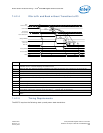
Power-State Transitions Timing — Intel
®
82575EB Gigabit Ethernet Controller
324632-003 Intel
®
82575EB Gigabit Ethernet Controller
Revision: 2.1 Software Developer’s Manual and EEPROM Guide
January 2011 229
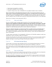
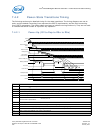
7.4.2.4 D0a to Dr and Back without Transition to D3
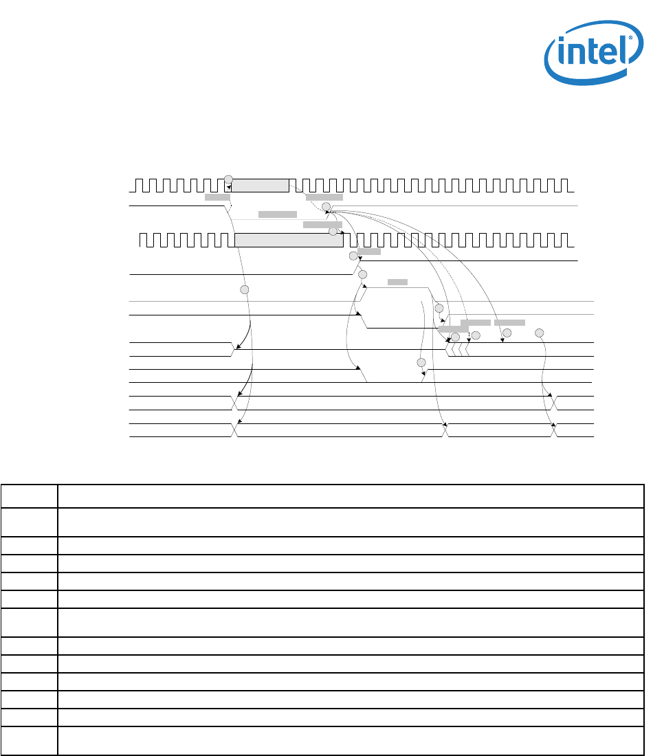
7.4.2.5 Timing Requirements
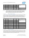
The 82575 requires the following start up and power state transitions.
Notes
1 The system must assert PE_RST_N before stopping the PCIe* reference clock. It must also wait t
l2clk
after link
transition to L2 or L3 before stopping the reference clock.
2 When PE_RST_N is asserted, the 82575 transitions to Dr state and the PCIe* link transitions to an electrical idle.
3 The system starts the PCIe* reference clock t
PWRGDPE_RST-CLK
before de-asserting PE_RST_N.
4 The internal PCIe* clock is valid and stable t
ppg-clkint
from PE_RST_N de-assertion.
5 The PCIe* internal PE_RST_N signal is asserted t
clkpr
after the external PE_RST_N signal.
6 Assertion of the internal PCIe* PE_RST_N causes the EEPROM to be re-read, asserts a PHY reset, and disables wake
up.
7 APM wake-up mode can be enabled based on the EEPROM contents.
8 After reading the EEPROM, PHY reset is de-asserted.
9 Link training starts after t
pgtrn
from PE_RST_N de-assertion.
10 A first PCIe* configuration access might arrive after t
pgcfg
from PE_RST_N de-assertion.
11 A first PCIe* configuration response can be sent after t
pgres
from PE_RST_N de-assertion.
12 Writing a 1b to the Memory Access Enable bit in the PCI Command Register transitions the 82575 from D0u to D0
state.
PCIe*
Reference Clock
PCIe* PwrGd
DState
PHY Power State
D0u
Reading EEPROM Read EEPROM
D0a
Power Managed Full
Reset to PHY
(Active Low)
PCIe* Link
Wakeup Enabled
Dr
8
Any Mode
APM/SMBus
Full
D0a
12
L0 L0
2
3
10
11
1
9
Internal PCIe*
Clock (2.5 GHz)
Internal PwrGd (PLL)
6
4
5
7
tee
tppg-clkint
tpgtrn
tpgres
tpgcfg
tclkpr
tpgdl
tclkpg
tPWRGD-CLK