


Register Descriptions — Intel
®
82575EB Gigabit Ethernet Controller
324632-003 Intel
®
82575EB Gigabit Ethernet Controller
Revision: 2.1 Software Developer’s Manual and EEPROM Guide
January 2011 287
14.0 Register Descriptions
This section details the state inside the 82575 that are visible to the programmer. In some cases, it
describes hardware structures invisible to software in order to clarify a concept.
The internal register/memory space is described in the following sections and divided up into the
following categories:
• General
• Interrupt
• MAC Receive
• MAC Transmit
• Statistics
• Wake Up
• PCIe*
• Diagnostics (including packet buffer memory access)
• Packet Generator
• PHY Receive, Transmit and Special Function
Note: The PHY registers are accessed through the MDI/O interface (see Section 14.3.8 for PHY
register descriptions).
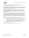
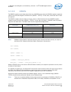
The 82575’s address space is mapped into five regions with PCI Base Address Registers described in the
table below. These regions are shown as follows.
Both the Flash and Expansion ROM Base Address Registers map the same Flash memory. The internal
registers and memories and Flash can be access through I/O space by doing a level of indirection, as
explained later.
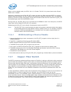
14.1 Register Conventions
All registers in the 82575 are defined to be 32 bits and should be accessed as 32-bit double words.
There are some exceptions to this rule:
Internal registers and memories (including PHY) Memory 128 KB
Flash (optional) Memory 64 - 512 KB
Expansion ROM (optional) Memory 64 - 512 KB
Internal registers and memories, Flash (optional) I/O Windows Mapped 32 Bytes
MSI-X (optional) Memory 16 KB