


PCI Power Management Registers — Intel
®
82575EB Gigabit Ethernet Controller
324632-003 Intel
®
82575EB Gigabit Ethernet Controller
Revision: 2.1 Software Developer’s Manual and EEPROM Guide
January 2011 207
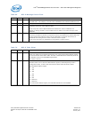
Link Status
The Link Status field is 2 bytes at offset B2h and is read only. This register provides information about
PCIe* link specific parameters. This is a read only register identical to all functions.
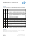
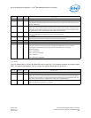
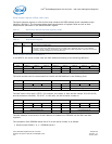
Bit(s) RD/WR Default Description
15:8 RO 0h Reserved
7 RW 0b Extended Synchronization
This bit forces extended transmit of the FTS ordered set in FTS and extra TS1 at exit from L0s
prior to entering L0.
6 RW 0b Common Clock Configuration
When this is set, it indicates that the 82575 and the component at the other end of the link are
operating with a common reference clock. A value of 0b indicates that they are operating with
an asynchronous clock. This parameter affects the L0s exit latencies.
5 RO 0b Retrain Clock
This is not applicable for endpoint devices and is hardwired to 0b.
4 RO 0b Link Disable
This field is not applicable for endpoint devices and is hardwired to 0b.
3 RW 0b Read Completion Boundary.
2 RO 0b Reserved
1:0 RW 00b Active State Link PM Control
This field controls the active state power management supported on the link. Link PM
functionality is determined by the lowest common denominator of all functions.
Defined encoding:
00b = PM disabled
01b = L0s entry supported
10b = Reserved
11b = L0s and L1 supported
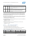
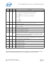
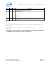
Bit(s) RD/WR Default Description
15:13 RO 0000b Reserved
12 HwInit 1b Slot Clock Configuration
When this is set, it indicates that the 82575 uses the physical reference clock that the platform
provides on the connector. This bit must be cleared if the 82575 uses an independent clock. The
Slot Clock Configuration bit is loaded from the Slot_Clock_Cfg EEPROM bit.
11 RO 0b Link Training
This indicates that link training is in progress.