


Intel
®
82575EB Gigabit Ethernet Controller — Power-State Transitions Timing
Intel
®
82575EB Gigabit Ethernet Controller 324632-003
Software Developer’s Manual and EEPROM Guide Revision: 2.1
228 January 2011
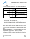
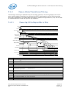
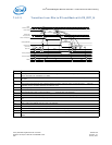
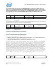
7.4.2.3 Transition from D0a to D3 and Back with PE_RST_N
Notes
1 Writing 11b to the Power State field of the Power Management Control/Status Register (PMCSR) transitions the 82575
to D3. The PCIe* link transitions to L1 state.
2 The system can delay an arbitrary amount of time between setting the D3 mode and transitioning the link to an L2 or
L3 state.
3 After a link transition, PE_RST_N is asserted.
4 The system must assert PE_RST_N before stopping the PCIe* reference clock. It must also wait t
l2clk
after link
transition to L2 or L3 before stopping the reference clock.
5 When PE_RST_N is asserted, the 82575 transitions to Dr state.
6 The system starts the PCIe* reference clock t
PWRGDPE_RST-CLK
before de-asserting PE_RST_N.
7 The internal PCIe* clock is valid and stable t
ppg-clkint
from PE_RST_N de-assertion.
8 The PCIe* internal PE_RST_N signal is asserted t
clkpr
after the external PE_RST_N signal.
9 Assertion of the internal PCIe* PE_RST_N causes the EEPROM to be re-read, asserts a PHY reset, and disables wake
up.
10 APM wake-up mode might be enabled based on the EEPROM contents.
11 After reading the EEPROM, the PHY reset is de-asserted.
12 Link training starts after t
pgtrn
from PE_RST_N de-assertion.
13 A first PCIe* configuration access might arrive after t
pgcfg
from PE_RST_N de-assertion.
14 A first PCIe* configuration response can be sent after t
pgres
from PE_RST_N de-assertion.
15 Writing a 1b to the Memory Access Enable bit in the PCI Command Register transitions the 82575 from D0u to D0
state.
PCIe*
Reference Clock
PCIe* PwrGd
DState
PHY Power State
D0u
Reading EEPROM Read EEPROM
D0a
Power Managed Full
Reset to PHY
(active low)
PCIe* Link
Wakeup Enabled
Dr
11
Any Mode
APM/SMBus
Full
D3 Write
D0a D3
15
L0 L1 L2/L3 L0
1
2
6
13
14
3
4a
4b
12
Internal PCIe*
Clock (2.5 GHz)
Internal PwrGd (PLL)
9
7
8
10
tee
tppg-clkint
tpgtrn
tpgres
tpgcfg
tclkpr
tpgdl
tl2clk
tclkpg
tPWRGD-CLK
tl2pg
5
L0