


Intel
®
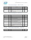
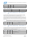
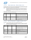
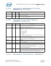
82575EB Gigabit Ethernet Controller — Packet Buffer Size - PBS (01008h; R/W)
Intel
®
82575EB Gigabit Ethernet Controller 324632-003
Software Developer’s Manual and EEPROM Guide Revision: 2.1
332 January 2011
14.3.19 Packet Buffer Size - PBS (01008h; R/W)
This register sets the on-chip receive and transmit storage allocation size, The allocation value is read/
write for the lower 6 bits. These legal values must be 8 KB aligned (the least 3 bits are 0b). The division
between transmit and receive is done according to the PBA register.
Note: Programming this register does not automatically re-load or initialize internal packet-buffer
RAM pointers. Software must reset both the transmit and receive operation (using the
global device reset CTRL.RST bit) after changing this register in order for it to take effect.
The PBS register itself is not reset by asserting global reset, but is only reset upon initial
hardware power-on.
Programming this register should be aligned with programming the PBA register hardware operation (if
PBA and PBS are not coordinated and not determined).
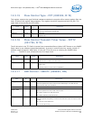
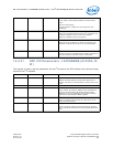
14.3.20 SFP 12C Command - I2CCMD (01028h; R/W)
This register is used by software to read or write to the EEPROM’s SFP modules.
Note: According to the SFP specification, only reads are allowed from this interface; however, SFP
vendors also provide a writable register through this interface (for example, PHY registers).
As a result, write capability is also supported.
Field Bit(s) Initial Value Description
PBS 15:0 0030h Packet Buffer Size in KB
This value must be a multiple of 8 KB. The upper 10 bytes
are always 0b. The default value is 48. The PBA register
defines how the packet buffer is allocated between transmit
and receive.
Reserved 30:16 0000h Reserved
Reads as 0b.
PB_MNG 31 0b Packet Buffer for Manageability
When set to 1b, all Rx/Tx traffic is not written to the packet
buffer so that the packet buffer could be used as memory
for manageability controller code.
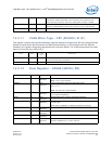
Field Bit(s) Initial Value Description
DATA 15:0 X Data
In a write command, software places the data bits and then
the MAC shifts them out to the I
2
C bus. In a read command,
the MAC reads these bits serially from the I
2
C bus and then
software reads them from this location.
Note: This field is read in byte order not in word order.
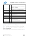
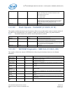
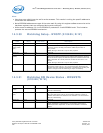
REGADD 23:16 0h I
2
C Register Address
For example, register 0, 1, 2, . . . 255.
PHYADD 26:24 0h Device Address Bits 1-3
The actual address used is b{1010, PHYADD[2:0], 0}.
OP 27 0b Op Code
0b = I
2
C write.
1b = I
2
C read.