


Section 3 DSP Operation
Rev. 4.00 Sep. 14, 2005 Page 133 of 982
REJ09B0023-0400
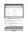
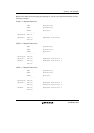
Table 3.18 Summary of DSP Data Transfer Instructions
X and Y Data Transfer
Operation (MOVX.W and
MOVY.W)
Single Data Transfer Operation
(MOVS.W and MOVS.L)
Address registers Ax: R4 and R5, Ay: R6 and R7 As: R2, R3, R4 and R5
Index register(s) Ix: R8, Iy: R9 Is: R8
Addressing
operations
Not update/Increment (+2)/
Add-index-register
Post-update
Not update/Increment (+2)/
Add-index-register
Post-update
Decrement (–2, –4): Pre-update
Modulo addressing Yes No
Data bus XDB and YDB LDB
Data length 16 bits (word) 16 bits/32 bits (word/longword)
Bus conflict No Possible (same as the SH)
Memory X and Y data memories All memory spaces
Source registers Dx, Dy: A0 and A1 DS: A0/A1, M0/M1, X0/X1, Y0/Y1, A0G,
A1G
Destination registers Dx: X0/X1, Dy: Y0/Y1 Ds: A0/A1, M0/M1, X0/X1, Y0/Y1, A0G,
A1G
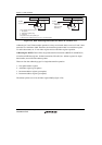
Addressing for MOVX.W and MOV.W: This LSI can access X and Y data memories
simultaneously (MOVX.W and MOVY.W). The DSP instructions have two address pointers that
simultaneously access X and Y data memories. The DSP instruction has only pointer-addressing
(it does not have immediate-addressing). Address registers are divided into two sets, R4 and R5
(Ax: Address register for X memory) and R6 and R7 (Ay: Address register for Y memory). There
are three data addressing types for X and Y data transfer instructions.
1. Not-update address register
2. Add-index register
3. Increment address register
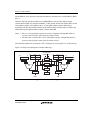
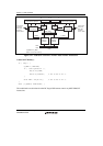
Each address pointer set has an index register, R8[Ix] for set Ax, and R9[Iy] for set Ay. Address
instructions for set Ax use ALU in the CPU, and address instructions for set Ay use a different
address unit (figure 3.19).