Section 16 I
2
C Bus Interface 2 (IIC2)
Rev. 4.00 Sep. 14, 2005 Page 475 of 982
REJ09B0023-0400
VccQ* VccQ*
SCL in
SCL out
SCL
SDA in
SDA out
SDA
SCL
(Master)
(Slave 1)
(Slave 2)
SDA
SCL in
SCL out
SCL
SDA in
SDA out
SDA
SCL in
SCL out
SCL
SDA in
SDA out
SDA
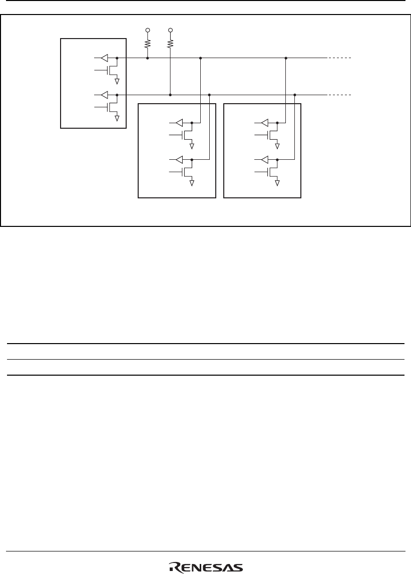
Note: * The I
2
C bus power supply and this LSI's power supply (VccQ)
must be switched ON or OFF simultaneously.
Figure 16.2 External Circuit Connections of I/O Pins
16.2 Input/Output Pins
Table 16.1 shows the pin configuration for the I
2
C bus interface 2.
Table 16.1 I
2
C Bus Interface Pin Configuration
Name Abbreviation I/O Function
Serial clock SCL I/O IIC serial clock input/output
Serial data SDA I/O IIC serial data input/output


