Section 12 Bus State Controller (BSC)
Rev. 4.00 Sep. 14, 2005 Page 356 of 982
REJ09B0023-0400
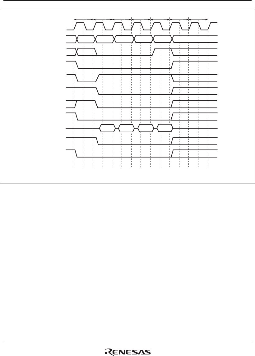
Tc4 TapTr Tc2 Tc3Tc1 Trwl
CKIO
A25 to A0
CSn
RD/WR
RASL, RASU
DQMxx
D31 to D0
BS
DACKn*
2
A12/A11*
1
CASL, CASU
Notes: 1. Address pin to be connected to pin A10 of SDRAM.
2. The waveform for DACKn is when active low is specified.
Figure 12.21 Basic Timing for Burst Write (Auto Pre-Charge)


