Section 12 Bus State Controller (BSC)
Rev. 4.00 Sep. 14, 2005 Page 363 of 982
REJ09B0023-0400
Tnop
Tc1
CKIO
A25 to A0
CSn
RD/WR
RASL, RASU
DQMxx
D31 to D0
BS
DACKn*
2
A12/A11*
1
CASL, CASU
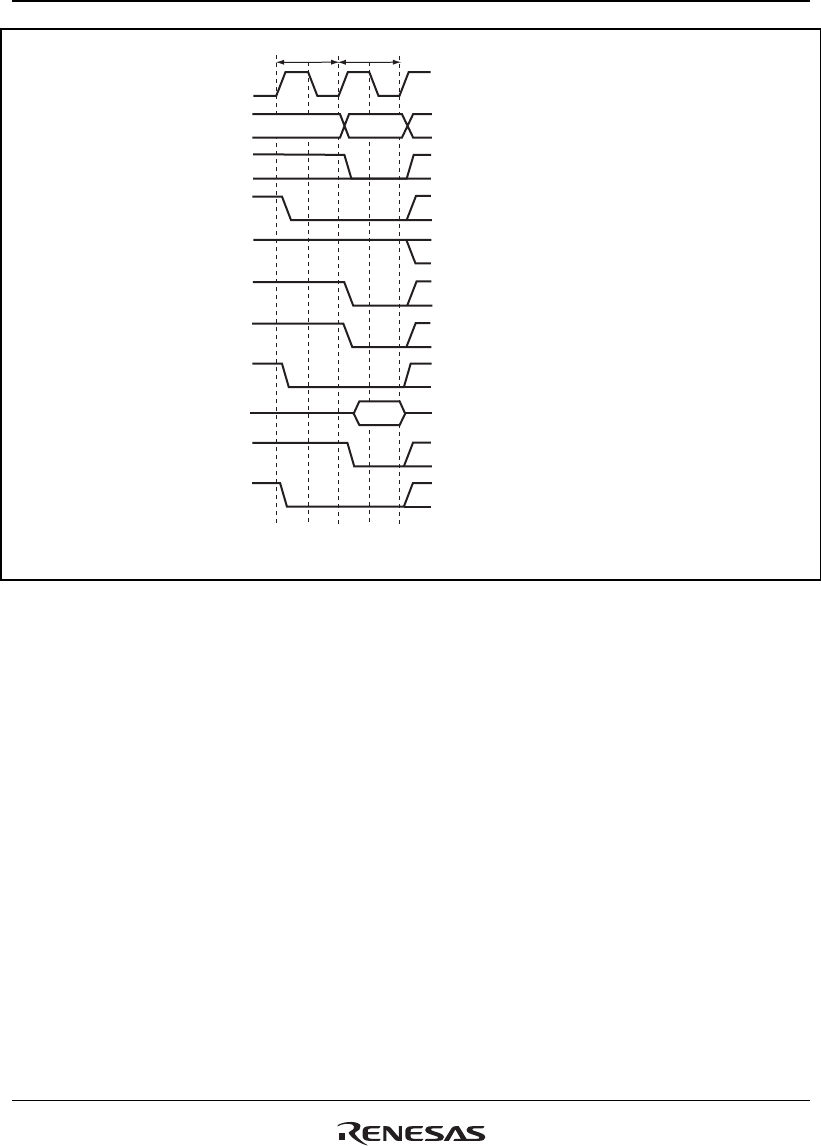
Notes: 1. Address pin to be connected to pin A10 of SDRAM.
2. The waveform for DACKn is when active low is specified.
Figure 12.27 Single Write Timing (Bank Active, Same Row Addresses in the Same Bank)


