Section 20 USB Function Module
Rev. 4.00 Sep. 14, 2005 Page 748 of 982
REJ09B0023-0400
• Power mode: Self-powered, bus-powered
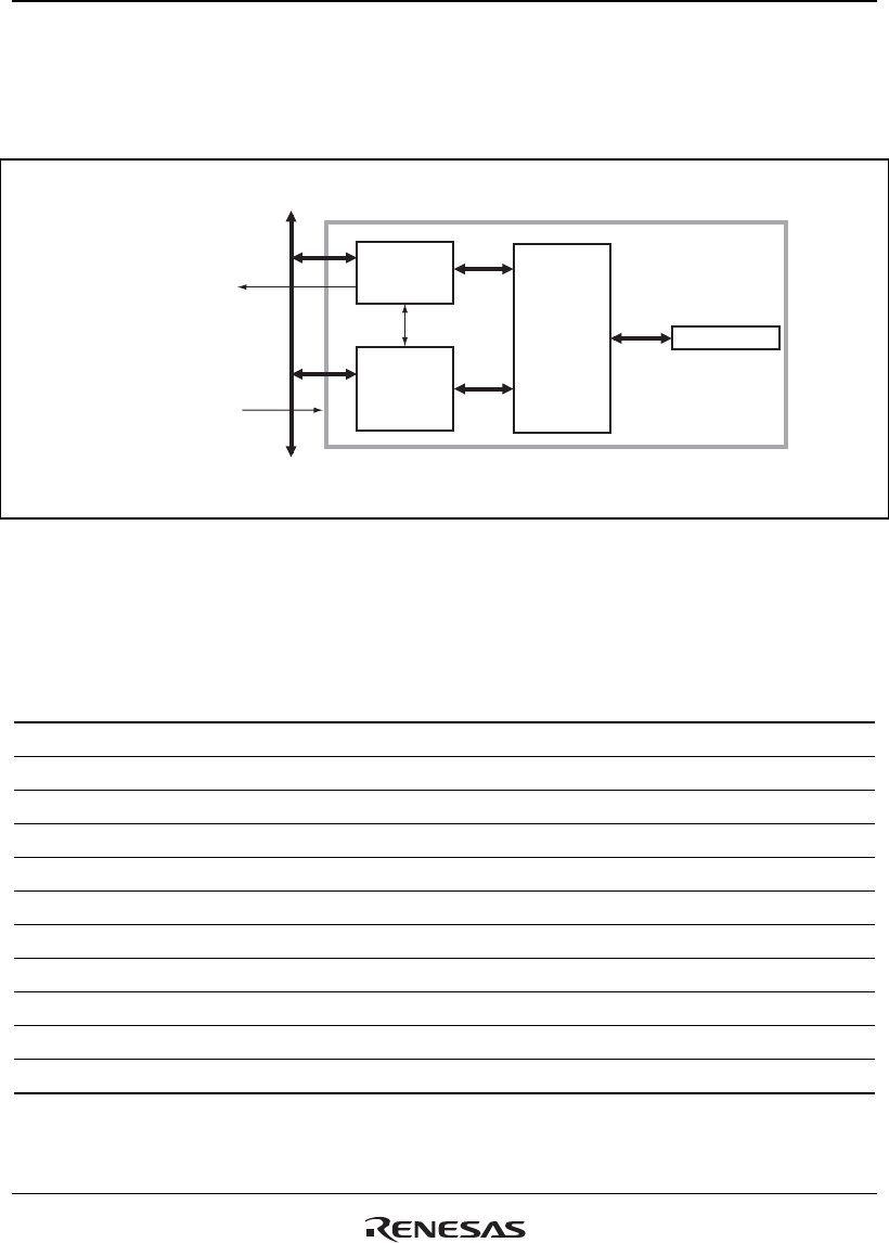
20.1.1 Block Diagram
Status
and control
registers
Internal
peripheral bus
UDC: USB device controller
FIFO
(288 bytes)
Interrupt requests
DMA transfer requests
Clock (48 MHz)
UDC
USB function module
To transceiver
Figure 20.1 Block Diagram of USB
20.2 Pin Configuration
Table 20.1 Pin Configuration and Functions
Pin Name I/O Function XVEROFF Conditions
XVDATA Input Input pin for receive data from differential receiver 1
DPLS Input Input pin to driver for D+ signal from receiver 1
DMNS Input Input pin to driver for D– signal from receiver 1
TXDPLS Output D+ transmit output pin to driver 1
TXDMNS Output D– transmit output pin to driver 1
TXENL Output Driver output enable pin 1
VBUS Input USB cable connection monitor pin 1/0
SUSPND Output Transceiver suspend state output pin 1/0
UCLK Input USB clock input pin (48 MHz input) 1/0
DP I/O On-chip transceiver D + signal 0
DM I/O On-chip transceiver D - signal 0


