


Section 18 Multi-Function Timer Pulse Unit (MTU)
Rev. 4.00 Sep. 14, 2005 Page 613 of 982
REJ09B0023-0400
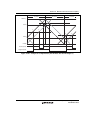
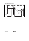
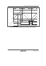
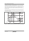
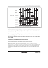
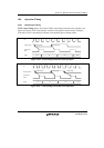
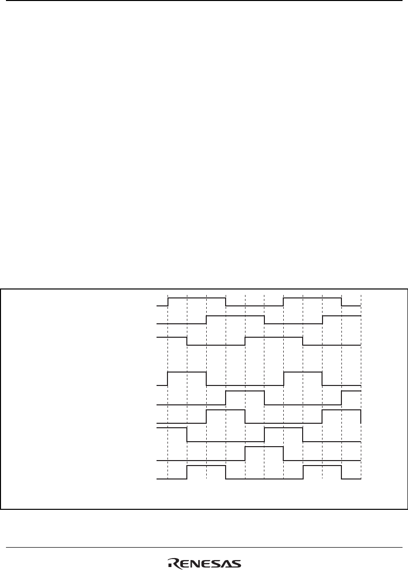
Example of AC Synchronous Motor (Brushless DC Motor) Drive Waveform Output: In
complementary PWM mode, a brushless DC motor can easily be controlled using the timer gate
control register (TGCR). Figures 18.50 to 18.53 show examples of brushless DC motor drive
waveforms created using TGCR.
When output phase switching for a 3-phase brushless DC motor is performed by means of external
signals detected with a Hall element, etc., clear the FB bit in TGCR to 0. In this case, the external
signals indicating the polarity position are input to channel 0 timer input pins TIOC0A, TIOC0B,
and TIOC0C (set with PFC). When an edge is detected at pin TIOC0A, TIOC0B, or TIOC0C, the
output on/off state is switched automatically.
When the FB bit is 1, the output on/off state is switched when the UF, VF, or WF bit in TGCR is
cleared to 0 or set to 1.
The drive waveforms are output from the complementary PWM mode 6-phase output pins. With
this 6-phase output, in the case of on output, it is possible to use complementary PWM mode
output and perform chopping output by setting the N bit or P bit to 1. When the N bit or P bit is 0,
level output is selected.
The 6-phase output active level (on output level) can be set with the OLSN and OLSP bits in the
timer output control register (TOCR) regardless of the setting of the N and P bits.
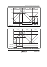
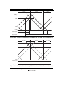
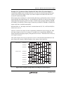
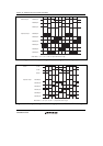
External input TIOC0A pin
TIOC0B pin
TIOC0C pin
TIOC3B pin
TIOC3D pin
TIOC4A pin
TIOC4C pin
TIOC4B pin
TIOC4D pin
6-phase output
When BCD = 1, N = 0, P = 0, FB = 0, output active level = high
Figure 18.50 Example of Output Phase Switching by External Input (1)