


Section 25 Electrical Characteristics
Rev. 4.00 Sep. 14, 2005 Page 920 of 982
REJ09B0023-0400
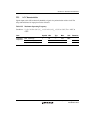
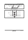
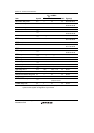
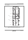
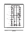
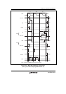
25.3.2 Control Signal Timing
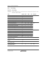
Table 25.7 Control Signal Timing
Conditions: V
CC
Q = 3.0 V to 3.6 V, V
CC
= 1.8 V ±5%, AV
CC
= 2.7 V to 3.6 V, V
SS
Q = V
SS
=
AV
SS
= 0 V, Ta = −40°C to +85°C
Bφ = 50 MHz*
2
Item Symbol Min. Max. Unit Figure(s)
RESETP pulse width t
RESPW
20*
2
— Bcyc*
4
RESETP setup time*
1
t
RESPS
22 — ns
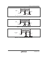
25.5, 25.6, 25.9, and
25.10
RESETP hold time t
RESPH
2 — ns
RESETM pulse width t
RESMW
12*
3
— Bcyc*
4
RESETM setup time t
RESMS
22 — ns
RESETM hold time t
RESMH
12 — ns
BREQ setup time t
BREQS
1/2t
cyc
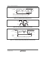
+ 10 — ns 25.11
BREQ hold time t
BREQH
1/2t
cyc
+ 10 — ns
NMI setup time*
1
t
NMIS
30 — ns 25.10
NMI hold time t
NMIH
30 — ns
IRQ7 to IRQ0 setup time*
1
t
IRQS
30 — ns
IRQ7 to IRQ0 hold time t
IRQH
30 — ns
BACK delay time t
BACKD
— 1/2t
cyc
+ 13 ns 25.11, 25.12
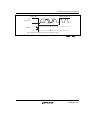
STATUS1, STATUS0 delay time t
STD
— 100 ns
Bus tri-state delay time 1 t
BOFF1
0 100 ns
Bus tri-state delay time 2 t
BOFF2
0 100 ns
Bus buffer on time 1 t
BON1
0 30 ns
Buss buffer on time 2 t
BON2
0 30 ns
Notes: 1. The RESETP, NMI and IRQ7 to IRQ0 signals are asynchronous signals. When the
setup time is satisfied, change of signal level is detected at the rising edge of the clock.
If not, the detection is delayed until the rising edge of the clock.
2. In standby mode, t
RESP
= t
OSC2
(10 ms). When multiplier of the clock is changed, t
REPW
= t
PLL1
(100 µs)
3. In standby mode, t
RESP
= t
OSC2
(10 ms). When multiplier of the clock is changed, RESETM
must be held low until signals STATUS0 and STATUS1 indicate the reset state (HH).
4. Bcyc indicates external clock cycle time. (B clock cycle)