Section 2 CPU
Rev. 4.00 Sep. 14, 2005 Page 35 of 982
REJ09B0023-0400
2.1.3 System Registers
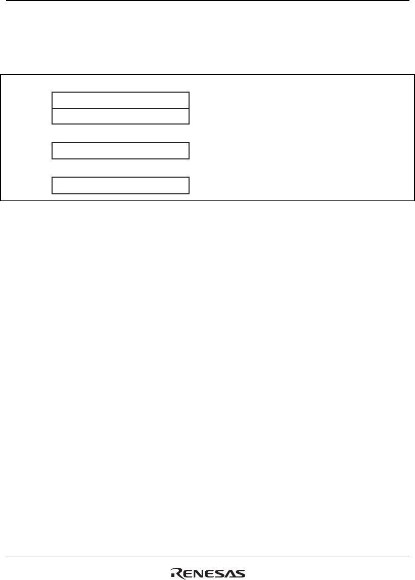
This LSI has four system registers, MACL, MACH, PR and PC (figure 2.6).
MACH
MACL
31
0
PR
31
0
PC
31
0
Multiply and accumulate high and low registers
(MACH and MACL)
Store the results of multiplicationand accumulation
operations.
Procedure register (PR)
Stores the subroutine procedure return address.
Program counter (PC)
Indicates the start address of the current instruction.
Figure 2.6 System Registers
The DSR, A0, X0, X1, Y0 and Y1 registers are also treated as system registers. Therefore,
instructions for data transfer between general registers and system registers are supported for these
registers.
2.1.4 DSP Registers
This LSI has eight data registers and one control register as DSP registers (figure 2.7). The data
registers are 32-bit width with the exception of registers A0 and A1. Registers A0 and A1 include
8 guard bits (fields A0G and A1G), giving them a total width of 40 bits.
Three kinds of operation access the DSP data registers. The first is DSP data processing. When a
DSP fixed-point data operation uses A0 or A1 as the source register, it uses the guard bits (bits 39
to 32). When it uses A0 or A1 as the destination register, guard bits 39 to 32 are valid. When a
DSP fixed-point data operation uses a DSP register other than A0 or A1 as the source register, it
sign-extends the source value to bits 39 to 32. When it uses one of these registers as the
destination register, bits 39 to 32 of the result are discarded.
The second kind of operation is an X or Y data transfer operation, "MOVX.W" or "MOVY.W".
This operation accesses the X and Y memories through the 16-bit X and Y data buses (figure 2.8).
The register to be loaded or stored by this operation always comprises the upper 16 bits (bits 31 to
16). X0 or X1 can be the destination of an X memory load and Y0 or Y1 can be the destination of
a Y memory load, but no other register can be the destination register in this operation.


