


Section 12 Bus State Controller (BSC)
Rev. 4.00 Sep. 14, 2005 Page 373 of 982
REJ09B0023-0400
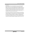
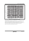
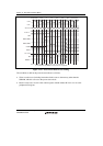
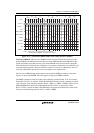
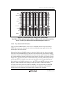
Tpw
Tp
Trr
Trc Trc
Tmw
Hi-Z
TnopTrc
Trr
Trc
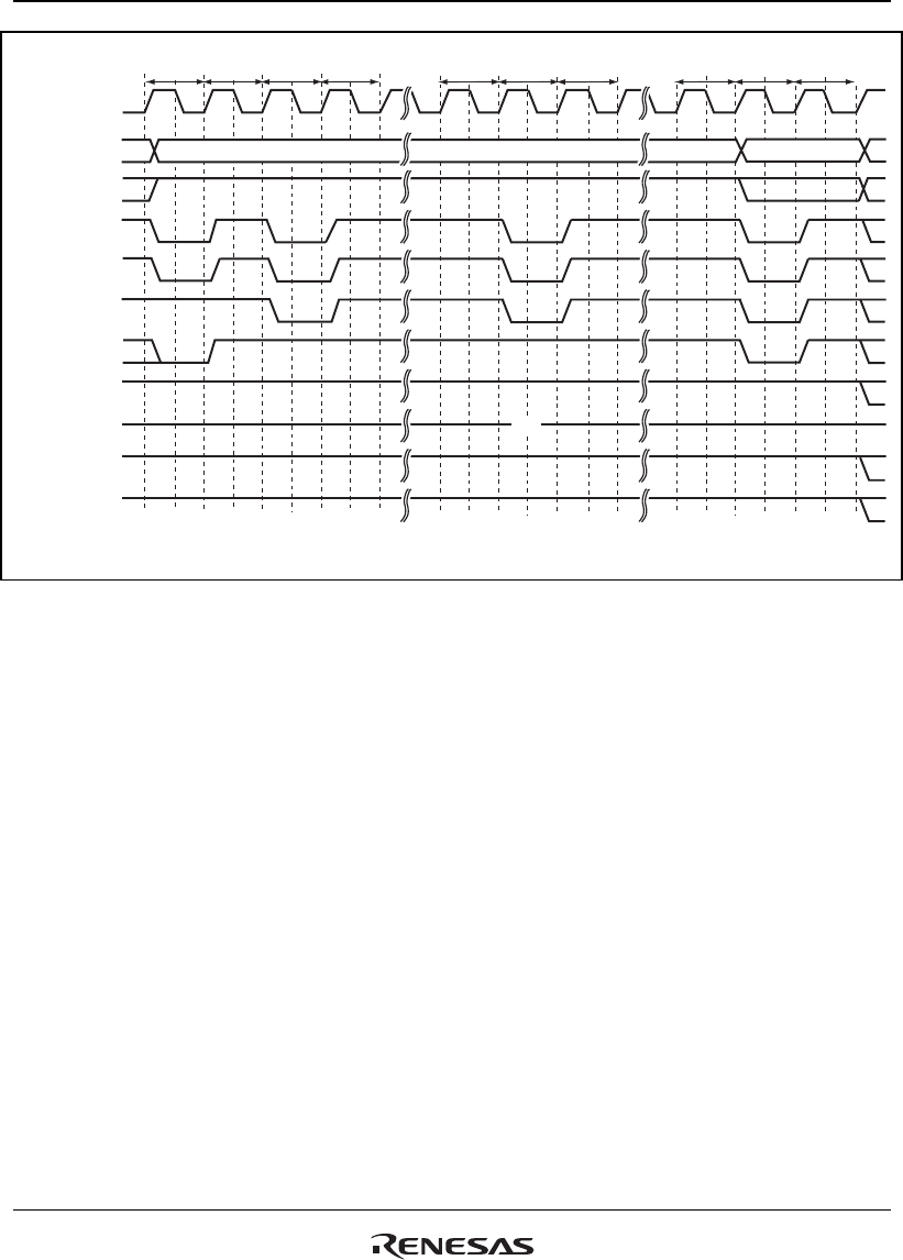
REF REF MRSPALL
CKIO
A25 to A0
CSn
RD/WR
RASL, RASU
DQMxx
D31 to D0
BS
DACKn*
2
A12/A11*
1
CASL, CASU
Notes: 1. Address pin to be connected to pin A10 of SDRAM.
2. The waveform for DACKn is when active low is specified.
Figure 12.33 Synchronous DRAM Mode Write Timing (Based on JEDEC)
Low-Power SDRAM: The low-power SDRAM can be accessed using the same protocol as the
normal SDRAM. The differences between the low-power SDRAM and normal SDRAM are that
partial refresh takes place that puts only a part of the SDRAM in the self-refresh state during the
self-refresh function, and that power consumption is low during refresh under user conditions such
as the operating temperature. The partial refresh is effective in systems in which there is data in a
work area other than the specific area can be lost without severe repercussions.
The low-power SDRAM supports the extension mode register (EMRS) in addition to the mode
registers as the normal SDRAM. This LSI supports issuing of the EMRS command.
The EMRS command is issued according to the conditions specified in table 12.21. For example,
if data H'0YYYYYYY is written to address H'A4FD5XX0 in longword, the commands are issued
to the CS3 space in the following sequence: PALL -> REF × 8 -> MRS -> EMRS. In this case, the
MRS and EMRS issue addresses are H'0000XX0 and H'YYYYYYY, respectively. If data
H'1YYYYYYY is written to address H'A4FD5XX0 in longword, the commands are issued to the
CS3 space in the following sequence: PALL -> MRS -> EMRS.