Section 18 Multi-Function Timer Pulse Unit (MTU)
Rev. 4.00 Sep. 14, 2005 Page 674 of 982
REJ09B0023-0400
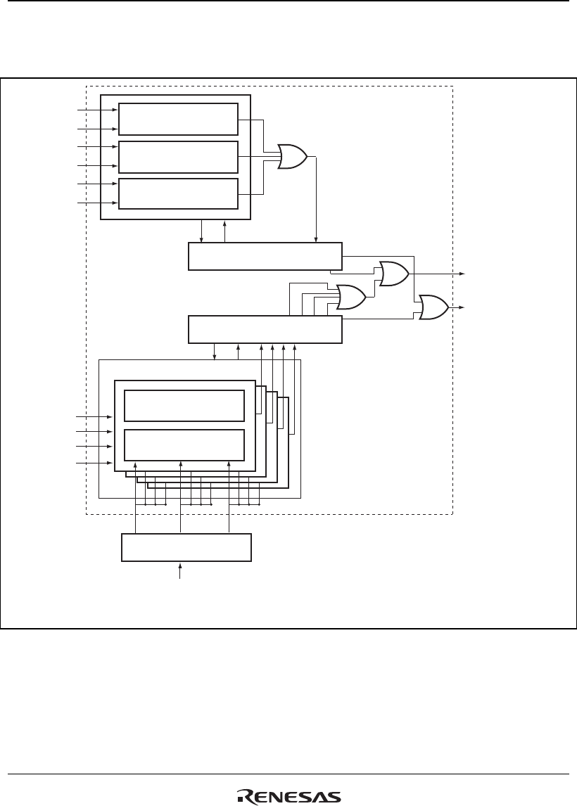
The POE has input-level detection circuitry and output-level detection circuitry, as shown in the
block diagram of figure 18.114.
TIOC3B
TIOC3D
TIOC4A
TIOC4C
TIOC4B
TIOC4D
POE3
POE2
POE1
POE0
Output level
detection circuit
Output level
detection circuit
Output level
detection circuit
Input level detection circuit
Falling-edge
detection circuit
Low-level
detection circuit
OCSR
Devider
ICSR1
φ/8 φ/16
pφ
φ/128
Hi-Z request
control signal
Interrupt request
[Legend]
OCSR: Output level control/status register
ICSR1: Input level control/status register
Figure 18.114 POE Block Diagram


