Section 13 Direct Memory Access Controller (DMAC)
Rev. 4.00 Sep. 14, 2005 Page 406 of 982
REJ09B0023-0400
• Transfer request acknowledge and transfer end signals: Active levels for DACK and TEND
can be set independently.
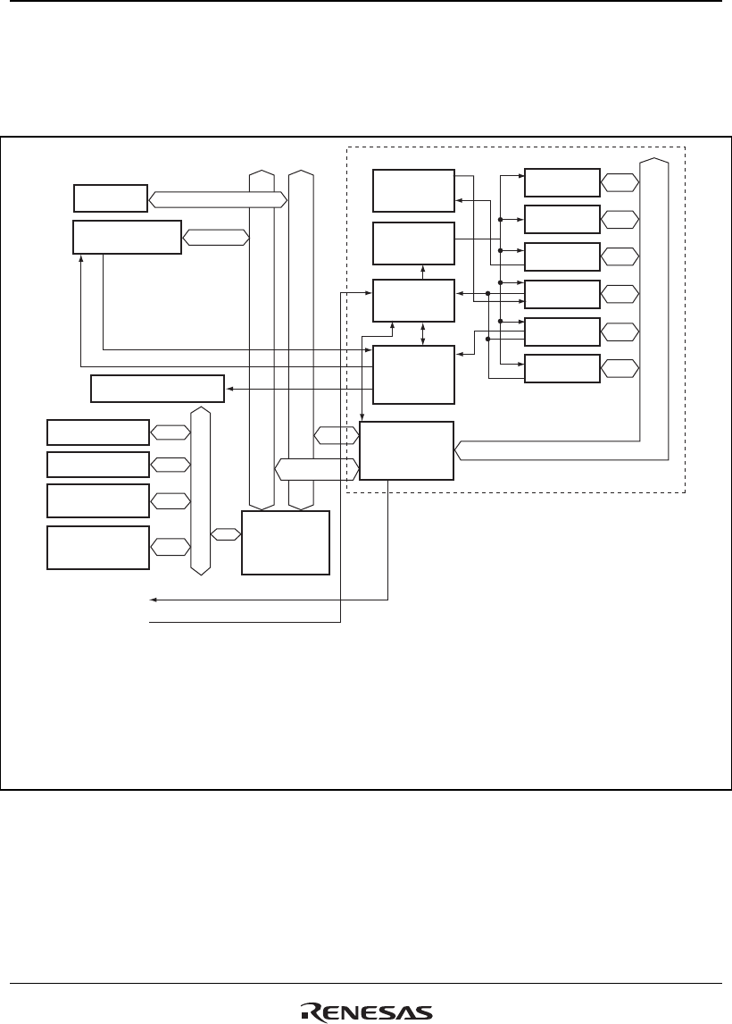
Figure 13.1 shows the block diagram of the DMAC.
On-chip
peripheral module
DMA transfer request signal
DMA transfer acknowledge signal
Peripheral bus
Internal bus
External ROM
X/Y memory
Interrupt controller
DREQ0 , DREQ1
DEIn
DACK0, DACK1
TEND
External RAM
Bus
interface
Bus state
controller
External device
(memory mapped)
External device
(with acknowledge-
ment)
Request
priority
control
Start-up
control
Register
control
Iteration
control
SAR_n
DAR_n
DMATCR_n
CHCR_n
DMAOR
DMARS0,1
[Legend]
SAR_n:
DAR_n:
DMATCR_n:
CHCR_n:
DMAOR:
DMARS0,1:
DEIn:
n:
DMA source address register
DMA destination address register
DMA transfer count register
DMA channel control register
DMA operation register
DMA extension resource selector
DMA transfer end interrupt request to the CPU
0, 1, 2, 3
DMAC module
Figure 13.1 Block Diagram of the DMAC


