Section 12 Bus State Controller (BSC)
Rev. 4.00 Sep. 14, 2005 Page 352 of 982
REJ09B0023-0400
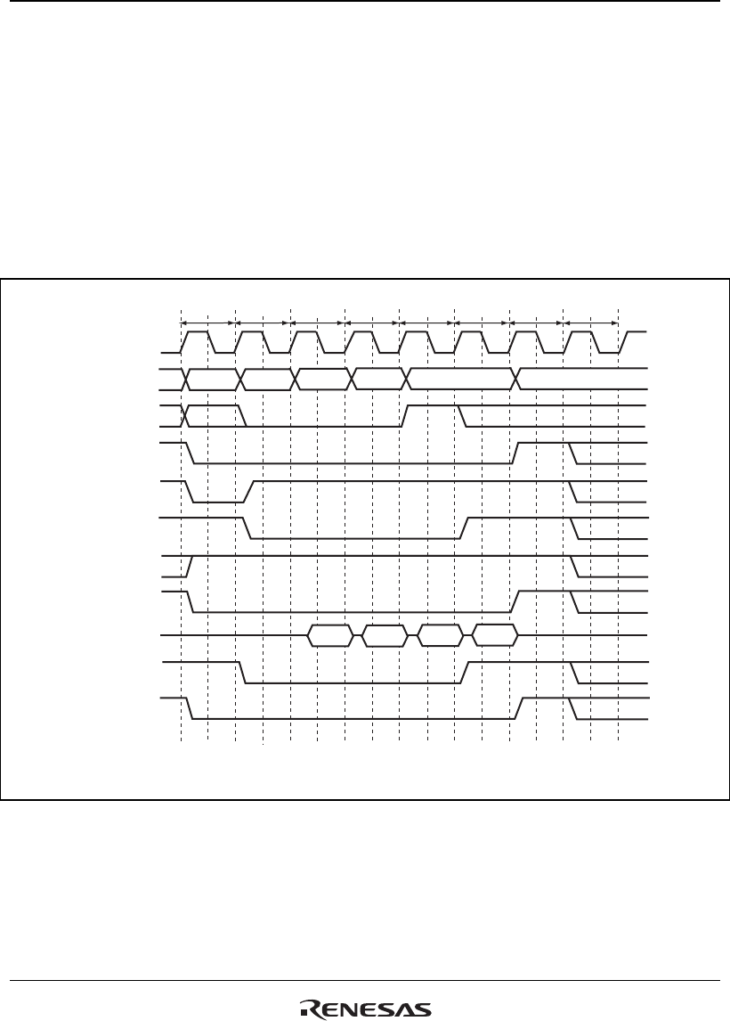
number of cycles from the Tc1 cycle where the READ command is output to the Td1 cycle where
the read data is latched can be specified for the CS2 and CS3 spaces independently, using the
A2CL1 and A2CL0 bits in the CS2WCR register or the A3CL1 and A3CL0 bits in the CS3WCR
register and WTRCD0 bit in the CS3WCR register. The number of cycles from Tc1 to Td1
corresponds to the SDRAM CAS latency. The CAS latency for the SDRAM is normally defined
as up to three cycles. However, the CAS latency in this LSI can be specified as 1 to 4 cycles. This
CAS latency can be achieved by connecting a latch circuit between this LSI and the SDRAM.
A Tde cycle is an idle cycle required to transfer the read data into this LSI and occurs once for
every burst read or every single read.
Tc4
CKIO
A25 to A0
CSn
RD/WR
RASL, RASU
DQMxx
D31 to D0
BS
(Tap)
DACKn*
2
Tr Tc2 Tc3
Tc1
Td4
Tde
Td2 Td3
Td1
A12/A11*
1
CASL, CASU
Notes: 1. Address pin to be connected to pin A10 of SDRAM.
2. The waveform for DACKn is when active low is specified.
Figure 12.18 Burst Read Basic Timing (CAS Latency 1, Auto Pre-Charge)


