


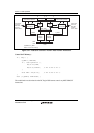
Section 4 Clock Pulse Generator (CPG)
Rev. 4.00 Sep. 14, 2005 Page 146 of 982
REJ09B0023-0400
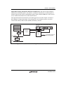
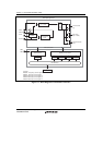
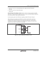
4.2 Input/Output Pins
Table 4.1 lists the CPG pins and their functions.
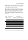
Table 4.1 Pin Configuration and Functions of the Clock Pulse Generator
Pin Name Symbol I/O
Function
(clock operating modes 2 and 6)
Function
(clock operating mode 7)
Mode control pins MD0 Input Set the clock operating mode.
MD2 Input Set the clock operating mode.
XTAL Output Connected to the crystal resonator (leave this pin open-circuit
when the crystal resonator is not in use).
Crystal input/output pins
(Clock input pins)
EXTAL Input Connected to the crystal resonator or used to input an external
clock.
Clock input/output pin CKIO I/O Clock output pin. The pin can also
be placed in the high-impedance
state.
Input for the external clock
pulse.
Clock-output pin CKIO2 Output Low-level output or clock output pin.
The selection is described in the
description of the common control
registers in section 12, Bus State
Controller (BSC).
High impedance
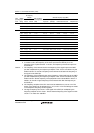
4.3 Clock Operating Modes
Table 4.2 shows the relationship between the mode control pins (MD2 and MD0) combinations
and the clock operating modes. Table 4.3 shows the usable frequency ranges in the clock operating
modes.
Table 4.2 Clock Operating Modes
Pin Values Clock I/O
Mode MD2 MD0 Source Output
PLL2
On/Off
PLL1
On/Off
CKIO Frequency
2 0 0 EXTAL or
Crystal resonator
CKIO ON (×4) ON (×1, 2) (EXTAL or
Crystal resonator) ×4
6 1 0 EXTAL or
Crystal resonator
CKIO ON (×2) ON (×1, 2, 3, 4) (EXTAL or
Crystal resonator) ×2
7 1 1 CKIO OFF ON (×1, 2, 3, 4) (CKIO)