Section 18 Multi-Function Timer Pulse Unit (MTU)
Rev. 4.00 Sep. 14, 2005 Page 630 of 982
REJ09B0023-0400
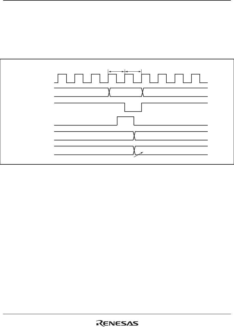
18.7.6 Conflict between TGR Write and Compare Match
When a compare match occurs in the T2 state of a TGR write cycle, the TGR write is executed
and the compare match signal is generated.
Figure 18.73 shows the timing in this case.
Compare
match signal
Write signal
Address
Pφ
TGR address
TCNT
TGR write cycle
T1
T2
NM
TGR write data
TGR
N N+1
Figure 18.73 Conflict between TGR Write and Compare Match
18.7.7 Conflict between Buffer Register Write and Compare Match
If a compare match occurs in the T1 state of a TGR write cycle, the data that is transferred to TGR
by the buffer operation differs depending on channel 0 and channels 3 and 4: data on channel 0 is
that after write, and on channels 3 and 4, before write.
Figures 18.74 and 18.75 show the timing in this case.


