Section 12 Bus State Controller (BSC)
Rev. 4.00 Sep. 14, 2005 Page 333 of 982
REJ09B0023-0400
T1
CKIO
A25 to A16
CSn
RD/WR
RD
D7 to D0 or
D15 to D0
WEn
D7 to D0 or
D15 to D0
BS
Read
Write
T2
DACKn*
Ta1 Ta2 Ta3
AH
Address
Address Data
Data
Tadw
Note: * The waveform for DACKn is when active low is specified.
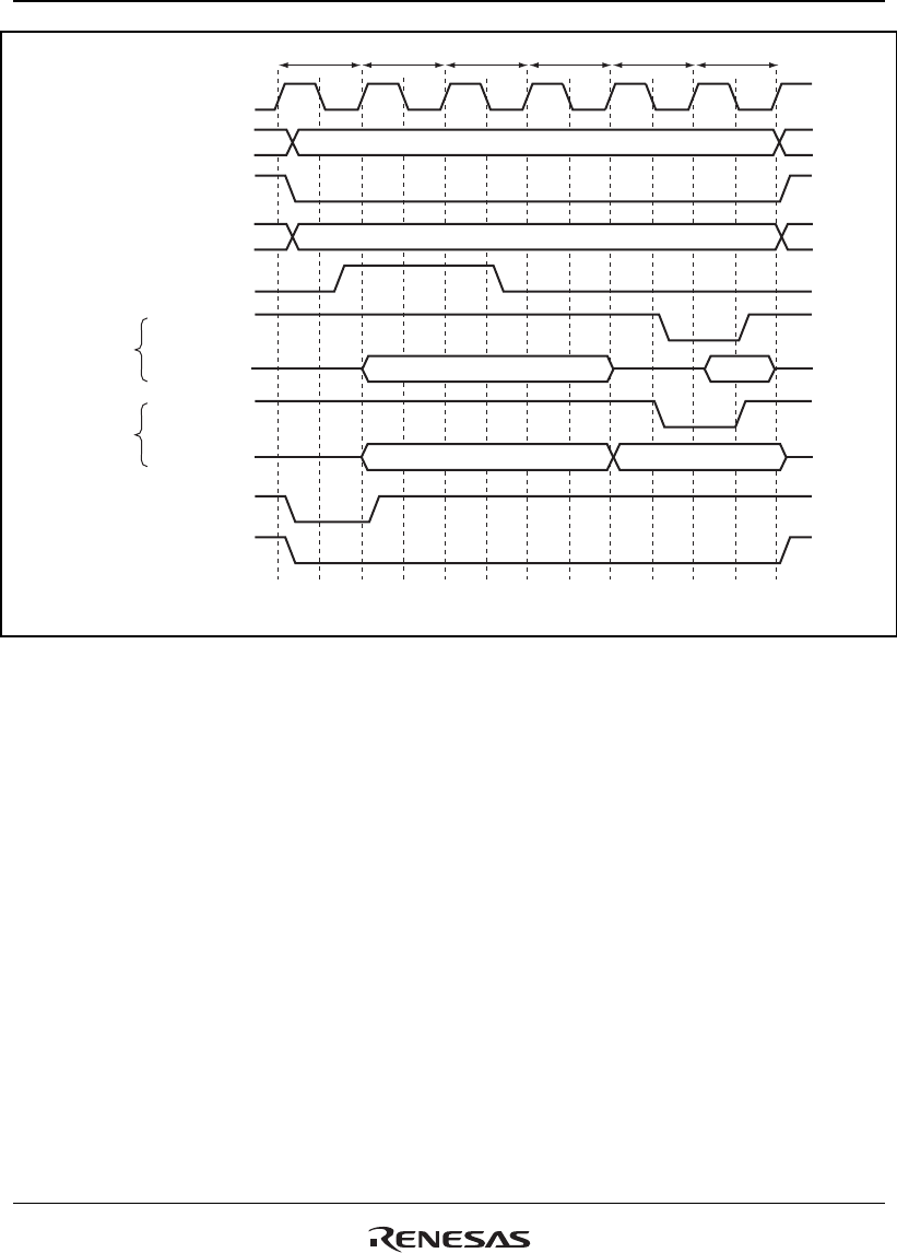
Figure 12.13 Access Timing for MPX Space (Address Cycle Wait 1, Data Cycle No Wait)


