


Section 1 Overview
Rev. 4.00 Sep. 14, 2005 Page 19 of 982
REJ09B0023-0400
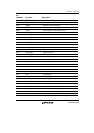
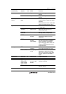
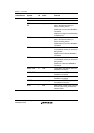
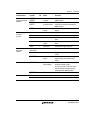
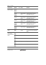
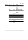
Classification Symbol I/O Name Function
CKIO O System clock Supplies the system clock to external
devices.
Clock
CKIO2 O System clock Supplies the system clock to external
devices.
Operating mode
control
MD3, MD2,
MD0
I Mode set Sets the operating mode. Do not
change values on these pins during
operation.
MD2, MD0 set the clock mode, MD3
set the bus-width mode of area 0.
RESETP I Power-on reset When low, this LSI enters the power-
on reset state.
RESETM I Manual reset When low, this LSI enters the
manual reset state.
STATUS1,
STATUS0
O Status output Indicate that this LSI is in software
standby, reset, or sleep mode.
BREQ I Bus-mastership
request
Low when an external device
requests the release of the bus
mastership.
System control
BACK O Bus-mastership
request
acknowledge
Indicates that the bus mastership
has been released to an external
device. Reception of the BACK
signal informs the device which has
output the BREQ signal that it has
acquired the bus.
NMI I Non-maskable
interrupt
Non-maskable interrupt request pin.
Fix to high level when not in use.
Interrupts
IRQ7 to IRQ0 I Interrupt requests
7 to 0
Maskable interrupt request pin.
Selectable as level input or edge
input. The rising edge, falling edge,
and both edges are selectable as
edges.
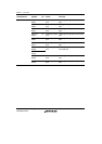
Address bus A25 to A0 O Address bus Outputs addresses.
Data bus D31 to D0 I/O Data bus 32-bit bidirectional bus.
CS0,
CS2 to CS4,
CS5A, CS5B,
CS6A, CS6B
O Chip select 0,
2 to 4, 5A, 5B,
6A, 6B
Chip-select signal for external
memory or devices.
Bus control
RD O Read Indicates reading of data from
external devices.