


Section 18 Multi-Function Timer Pulse Unit (MTU)
Rev. 4.00 Sep. 14, 2005 Page 598 of 982
REJ09B0023-0400
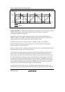
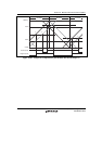
Initialization: In complementary PWM mode, there are six registers that must be initialized.
Before setting complementary PWM mode with bits MD3 to MD0 in the timer mode register
(TMDR), the following initial register values must be set.
TGRC_3 operates as the buffer register for TGRA_3, and should be set with 1/2 the PWM carrier
cycle + dead time Td. The timer cycle buffer register (TCBR) operates as the buffer register for
the timer cycle data register (TCDR), and should be set with 1/2 the PWM carrier cycle. Set dead
time Td in the timer dead time data register (TDDR).
Set the respective initial PWM duty values in buffer registers TGRD_3, TGRC_4, and TGRD_4.
The values set in the five buffer registers excluding TDDR are transferred simultaneously to the
corresponding compare registers when complementary PWM mode is set.
Set TCNT_4 to H'0000 before setting complementary PWM mode.
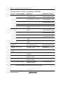
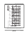
Table 18.41 Registers and Counters Requiring Initialization
Register/Counter Set Value
TGRC_3 1/2 PWM carrier cycle + dead time Td
TDDR Dead time Td
TCBR 1/2 PWM carrier cycle
TGRD_3, TGRC_4, TGRD_4 Initial PWM duty value for each phase
TCNT_4 H'0000
Note: The TGRC_3 set value must be the sum of 1/2 the PWM carrier cycle set in TCBR and
dead time Td set in TDDR.
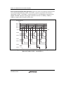
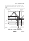
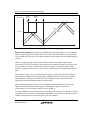
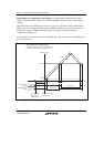
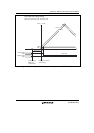
PWM Output Level Setting: In complementary PWM mode, the PWM pulse output level is set
with bits OLSN and OLSP in the timer output control register (TOCR).
The output level can be set for each of the three positive phases and three negative phases of 6-
phase output.
Complementary PWM mode should be cleared before setting or changing output levels.