Section 12 Bus State Controller (BSC)
Rev. 4.00 Sep. 14, 2005 Page 377 of 982
REJ09B0023-0400
CKIO
A25 to A0
RD
D15 to D0
DACKn*
Note: * The waveform for DACKn when active low is specified.
WAIT
CSn
T1 Tw Tw TB2 Twb TB2 Twb TB2 Twb T2
RD/WR
BS
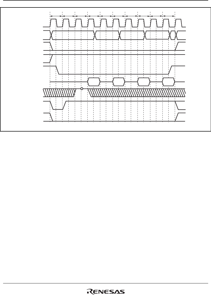
Figure 12.36 Burst ROM Access Timing (Clock Asynchronous)
(Bus Width = 32 Bits, 16-Byte Transfer (Number of Burst 4), Wait Cycles Inserted in First
Access = 2, Wait Cycles Inserted in Second and Subsequent Accesses = 1)
12.5.8 Byte-Selection SRAM Interface
The byte-selection SRAM interface is for access to an SRAM which has a byte-selection pin
(WEn). This interface has 16-bit data pins and accesses SRAMs having upper and lower byte
selection pins, such as UB and LB.
When the BAS bit in the CSnWCR register is cleared to 0 (initial value), the write access timing
of the byte-selection SRAM interface is the same as that for the normal space interface. While in
read access of a byte-selection SRAM interface, the byte-selection signal is output from the WEn
pin, which is different from that for the normal space interface. The basic access timing is shown
in figure 12.37. In write access, data is written to the memory according to the timing of the byte-
selection pin (WEn). For details, please refer to the Data Sheet for the corresponding memory.
If the BAS bit in the CSnWCR register is set to 1, the WEn pin and RD/WR pin timings change.
Figure 12.38 shows the basic access timing. In write access, data is written to the memory
according to the timing of the write enable pin (RD/WR). The data hold timing from RD/WR
negation to data write must be acquired by setting the HW1 and HW0 bits in the CSnWCR
register. Figure 12.39 shows the access timing when a software wait is specified.


