Section 12 Bus State Controller (BSC)
Rev. 4.00 Sep. 14, 2005 Page 400 of 982
REJ09B0023-0400
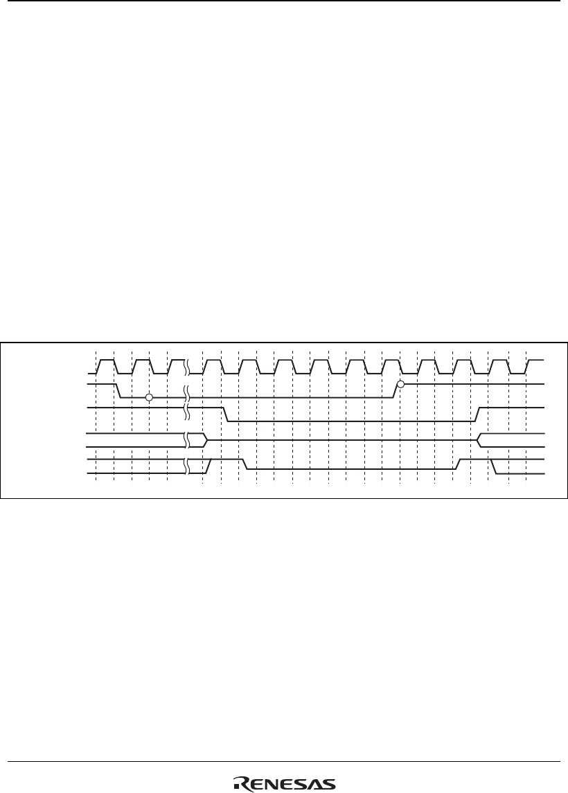
The sequence for reclaiming the bus mastership from an external device is described below. 1.5
cycles after the negation of BREQ is detected at the falling edge of CKIO, the bus control signals
are driven high. The bus enable signal is negated at the next falling edge of the clock. The fastest
timing at which actual bus cycles can be resumed after bus control signal assertion is at the rising
edge of the CKIO where address and data signals are driven. Figure 12.48 shows the bus
arbitration timing.
While releasing the bus mastership, the SLEEP instruction (to enter the sleep mode or the standby
mode), as well as a manual reset, cannot be executed until the LSI obtains the bus mastership. The
BREQ input signal is ignored in the standby mode and the BACK output signal are placed in the
high impedance state. If the bus mastership request is required in this state, the bus mastership
must be released by pulling down the BACK pin to enter the standby mode. The bus mastership
release (BREQ signal for high level negation) after the bus mastership request (BREQ signal for
low level assertion) must be performed after the bus usage permission (BACK signal for low level
assertion). If the BREQ signal is negated before the BACK signal is asserted, only one cycle of the
BACK signal is asserted depending on the timing of the BREQ signal to be negated and this may
cause a bus contention between the external device and the LSI.
CKIO
Other bus
contorol sigals
BREQ
BACK
A25 to A0
D31 to D0
CSn
Figure 12.48 Bus Arbitration Timing (Clock Mode 7 or CMNCR.HIZCNT = 1)


