


Section 18 Multi-Function Timer Pulse Unit (MTU)
Rev. 4.00 Sep. 14, 2005 Page 573 of 982
REJ09B0023-0400
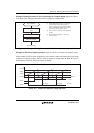
Examples of Buffer Operation:
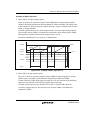
• When TGR is an output compare register
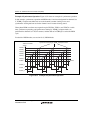
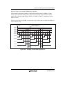
Figure 18.16 shows an operation example in which PWM mode 1 has been designated for
channel 0, and buffer operation has been designated for TGRA and TGRC. The settings used
in this example are TCNT clearing by compare match B, 1 output at compare match A, and 0
output at compare match B.
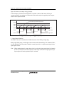
As buffer operation has been set, when compare match A occurs the output changes and the
value in buffer register TGRC is simultaneously transferred to timer general register TGRA.
This operation is repeated each time that compare match A occurs.
For details of PWM modes, see section 18.4.5, PWM Modes.
TCNT value
TGRB_0
H'0000
TGRC_0
TGRA_0
H'0200 H'0520
TIOCA
H'0200
H'0450
H'0520
H'0450
TGRA_0
H'0450
H'0200
Transfer
Time
Figure 18.16 Example of Buffer Operation (1)
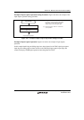
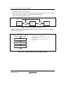
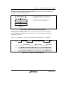
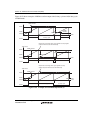
• When TGR is an input capture register
Figure 18.17 shows an operation example in which TGRA has been designated as an input
capture register, and buffer operation has been designated for TGRA and TGRC.
Counter clearing by TGRA input capture has been set for TCNT, and both rising and falling
edges have been selected as the TIOCA pin input capture input edge.
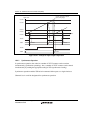
As buffer operation has been set, when the TCNT value is stored in TGRA upon the
occurrence of input capture A, the value previously stored in TGRA is simultaneously
transferred to TGRC.