


Section 12 Bus State Controller (BSC)
Rev. 4.00 Sep. 14, 2005 Page 277 of 982
REJ09B0023-0400
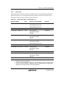
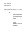
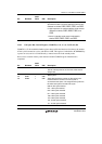
12.3.4 Area 0 Memory Type and Memory Bus Width
The memory bus width in this LSI can be set for each area. In area 0, external pins can be used to
select word (16 bits), or longword (32 bits) on power-on reset. The correspondence between the
external pin MD3 and memory size is listed in the table below.
Table 12.4 Correspondence between External Pin MD3 and Bus Width of Area 0
MD3 Bus Width of Area 0
0 16 bits
1 32 bits
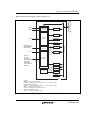
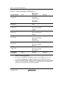
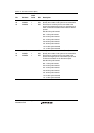
12.4 Register Descriptions
The BSC has the following registers. For the addresses and access sizes of these registers, see
section 24, List of Registers.
Do not access spaces other than CS0 until the termination of the setting the memory interface.
• Common control register (CMNCR)
• Bus control register for area 0 (CS0BCR)
• Bus control register for area 2 (CS2BCR)
• Bus control register for area 3 (CS3BCR)
• Bus control register for area 4 (CS4BCR)
• Bus control register for area 5A (CS5ABCR)
• Bus control register for area 5B (CS5BBCR)
• Bus control register for area 6A (CS6ABCR)
• Bus control register for area 6B (CS6BBCR)
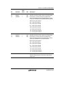
• Wait control register for area 0 (CS0WCR)
• Wait control register for area 2 (CS2WCR)
• Wait control register for area 3 (CS3WCR)
• Wait control register for area 4 (CS4WCR)
• Wait control register for area 5A (CS5AWCR)
• Wait control register for area 5B (CS5BWCR)
• Wait control register for area 6A (CS6AWCR)
• Wait control register for area 6B (CS6BWCR)
• SDRAM control register (SDCR)