Section 4 Clock Pulse Generator (CPG)
Rev. 4.00 Sep. 14, 2005 Page 153 of 982
REJ09B0023-0400
• A pair of Vss and Vcc for the input/output power supply nearest the USB module
H3 to H4
• A pair of Vss and Vcc for the A/D converter.
W19 to U20
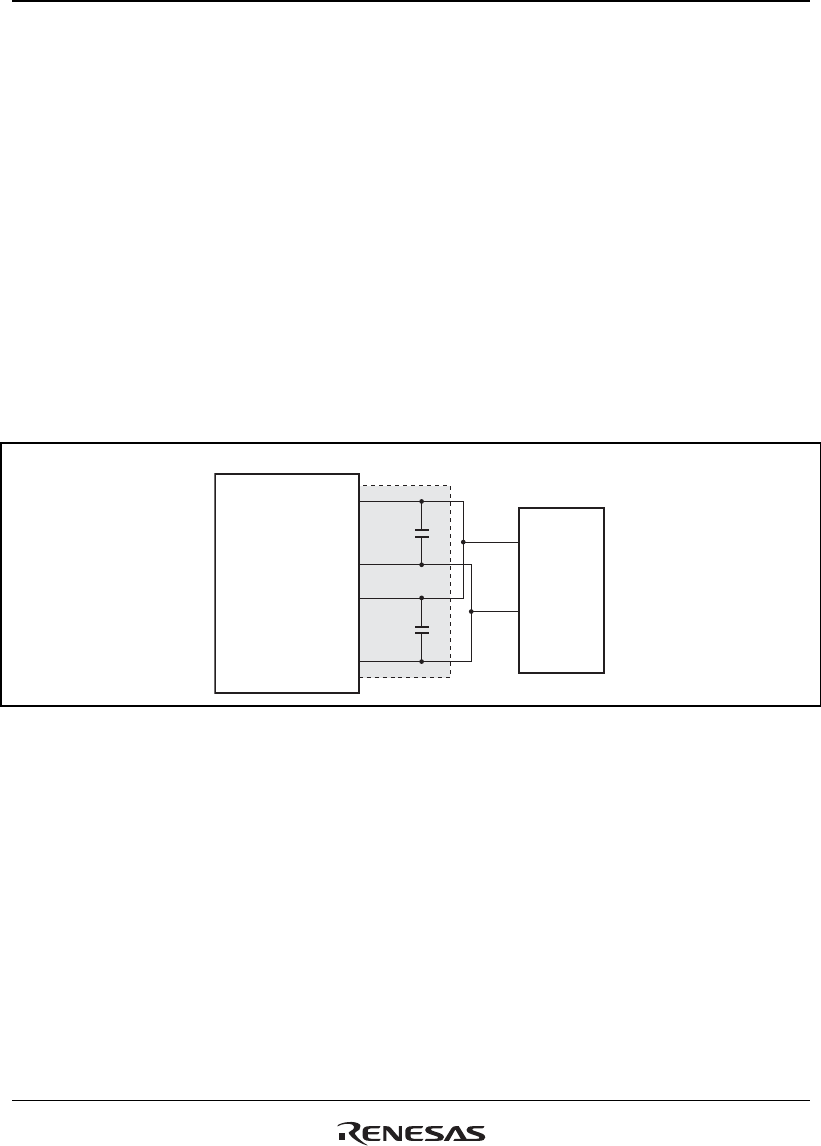
Notes on Using a PLL Oscillator Circuit: In the Vcc and Vss connection pattern for the PLL,
signal lines from the board power supply pins must be as short as possible and pattern width must
be as wide as possible to reduce inductive interference.
In clock operating mode 7, the EXTAL pin is pulled up and the XTAL pin is left open.
Since the analog power supply pins of the PLL are sensitive to the noise, the system may
malfunction due to inductive interference at the other power supply pins. To prevent such
malfunction, the analog power supply pin Vcc and digital power supply pin VccQ should not
supply the same resources on the board if at all possible.
Vcc(PLL2)
Vss(PLL2)
Vcc(PLL1)
Vss(PLL1)
Vcc
Vss
Power supply
Signal lines prohibited
Figure 4.3 Note on Using a PLL Oscillator Circuit


