


Section 6 Power-Down Modes
Rev. 4.00 Sep. 14, 2005 Page 172 of 982
REJ09B0023-0400
6.3.2 Standby Mode
1. Transition to Standby Mode
The LSI switches from a program execution state to a standby mode by executing the SLEEP
instruction when the STBY bit is 1 in STBCR register. In standby mode, not only the CPU but
also the clock and on-chip peripheral modules halt. The clock outputs from the CKIO and
CKIO2 pins also halt.
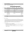
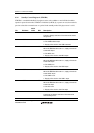
The contents of the CPU and cache registers remain unchanged. Some registers of on-chip
peripheral modules are, however, initialized. Table 6.3 lists the states of on-chip peripheral
modules registers in standby mode.
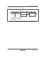
Table 6.3 Register States in Standby Mode
Module Registers Initialized Registers Retaining Data
Interrupt controller (INTC) All registers
On-chip clock pulse generator (CPG) All registers
User break controller (UBC) — All registers
Bus state controller (BSC) — All registers
A/D converter (ADC) All registers —
I/O port — All registers
H-UDI — All registers
SCIF — All registers
USB — All registers
MTU All registers —
POE — All registers
DMAC — All registers
CMT — All registers
IIC2 — All registers
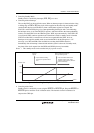
The procedure for switching to standby mode is as follows:
A. Clear the TME bit in the WDT's timer control register (WTCSR) to 0 to stop the WDT.
B. Set the WDT's timer counter (WTCNT) to 0 and the CKS2 to CKS0 bits in the WTCSR
register to appropriate values to secure the specified oscillation settling time.
C. After the STBY bit in the STBCR register is set to 1, a SLEEP instruction is executed.
D. Standby mode is entered and the clocks within the chip are halted. The STATUS1 and
STATUS0 pins output low and high, respectively.