Section 12 Bus State Controller (BSC)
Rev. 4.00 Sep. 14, 2005 Page 332 of 982
REJ09B0023-0400
12.5.5 MPX-I/O Interface
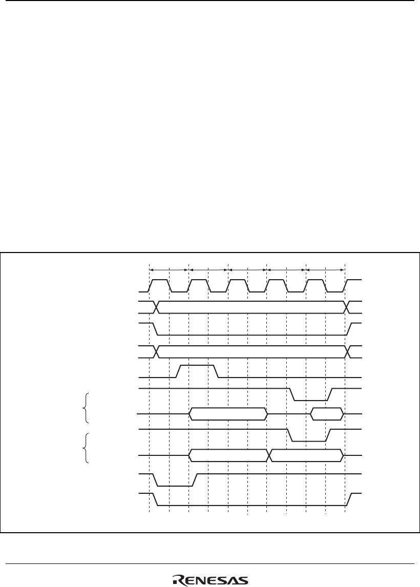
Access timing for the MPX space is shown below. In the MPX space, CS5B, AH, RD, and WEn
signals control the accessing. The basic access for the MPX space consists of 2 cycles of address
output followed by an access to a normal space. The bus width for the address output cycle or the
data input/output cycle is fixed to 8 bits or 16 bits. Alternatively, it can be 8 bits or 16 bits
depending on the address to be accessed.
Output of the addresses D15 to D0 or D7 to D0 is performed from cycle Ta2 to cycle Ta3.
Because cycle Ta1 has a high-impedance state, collisions of addresses and data can be avoided
without inserting idle cycles, even in continuous accesses. Address output is increased to 3 cycles
by setting the MPXW bit in the CS5BWCR register to 1. The RD/WR signal is output at the same
time as the CS5B signal; it is high in the read cycle and low in the write cycle.
The data cycle is the same as that in a normal space access.
Timing charts are shown in figures 12.12 to 12.14.
T1
CKIO
A25 to A16
CSn
RD/WR
RD
D7 to D0 or
D15 to D0
WEn
D7 to D0 or
D15 to D0
BS
Read
Write
T2
DACKn*
Ta1 Ta2 Ta3
AH
Address
Address Data
Data
Note: * The waveform for DACKn is when active low is specified.
Figure 12.12 Access Timing for MPX Space (Address Cycle No Wait, Data Cycle No Wait)


