Section 12 Bus State Controller (BSC)
Rev. 4.00 Sep. 14, 2005 Page 386 of 982
REJ09B0023-0400
Note: * The waveform for DACKn is when active low is specified.
CKIO
D31 to D0
A25 to A0
FRAME
CS6B
RD/WR
WAIT
BS
DACKn*
Tm1 Tmd1 Tmd2 Tmd3
Tmd4
A
D0
D1
D2
D3
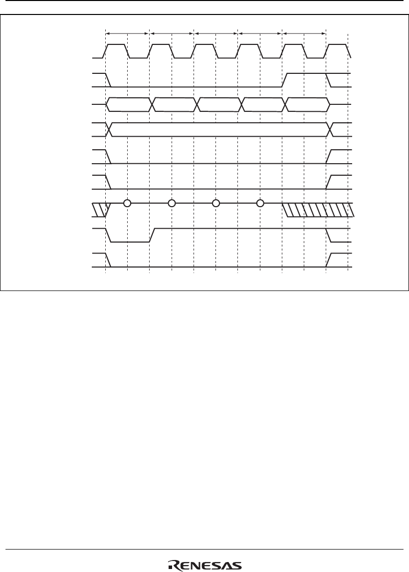
Figure 12.46 Burst MPX Space Access Timing
(Burst Write, No Wait, CS6BWCR.MPXMD = 0)
12.5.10 Burst ROM Interface (Clock Synchronous)
The burst ROM (clock synchronous) interface is supported to access a ROM with a synchronous
burst function at high speed. The burst ROM interface accesses the burst ROM in the same way as
a normal space. This interface is valid only for area 0.
In the first access cycle, wait cycles are inserted. In this case, the number of wait cycles to be
inserted is specified by the W3 to W0 bits in CS0WCR. In the second and subsequent cycles, the
number of wait cycles to be inserted is specified by the BW1 and BW0 bits in CS0WCR.
While the burst ROM is accessed (clock synchronous), the BS signal is asserted only for the first
access cycle and an external wait input is also valid for the first access cycle.
If the bus width is 16 bits, the burst length must be specified as 8. If the bus width is 32 bits, the
burst length must be specified as 4. The burst ROM interface does not support the 8-bit bus width
for the burst ROM.


