


Section 12 Bus State Controller (BSC)
Rev. 4.00 Sep. 14, 2005 Page 280 of 982
REJ09B0023-0400
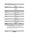
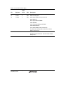
Bit Bit Name
Initial
Value R/W Description
5 DMAIWA 0 R/W Method of inserting wait states between access cycles
when DMA single address transfer is performed.
Specifies the method of inserting the idle cycles
specified by the DMAIW[2:0] bit. Clearing this bit will
make this LSI insert the idle cycles when another
device, which includes this LSI, drives the data bus
after an external device with DACK drove it. However,
when the external device with DACK drives the data
bus continuously, idle cycles are not inserted. Setting
this bit will make this LSI insert the idle cycles after an
access to an external device with DACK, even when
the continuous accesses to an external device with
DACK are performed.
0: Idle cycles inserted when another device drives the
data bus after an external device with DACK drove
it.
1: Idle cycles always inserted after an access to an
external device with DACK
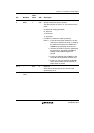
4 1 R Reserved
This bit is always read as 1. The write value should
always be 1.
3 0 R Reserved
This bit is always read as 0. The write value should
always be 0.
2 CKD2RDV 0 R CKIO2 Drive
Specifies whether the CKIO2 pin outputs a low level
signal or clock (Bφ). In clock mode 7 (CKIO pin input),
the CKIO2 pin has high impedance. The CK2DRV bit
setting is enabled in the 2 or 6 clock mode.
0: Outputs a low level signal
1: Outputs a clock (Bφ)
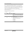
1 HIZMEM 0 R/W High-Z Memory Control
Specifies the pin state in software standby mode for
A25 to A0, BS, CS, RD/WR, WEn/DQNxx, RD, and
FRAME.
0: High impedance in standby mode.
1: Driven in standby mode