


Section 23 I/O Ports
Rev. 4.00 Sep. 14, 2005 Page 857 of 982
REJ09B0023-0400
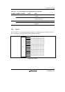
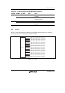
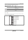
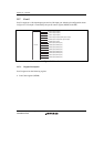
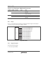
23.7.2 Port G Data Register (PGDR)
PGDR a register that includes six readable/writable and eight readable bits with two reserved bits
that store data for pins PTG13 to PTG0.
PGDR13 to PGDR8 are initialized to H'00 by a power-on reset, but they retain their previous
values by a manual reset, in standby mode, or in sleep mode. PGDR7 to PGDR0 are not initialized
by a power-on or manual reset, in standby mode, or in sleep mode. (The bit always indicates the
status of the pin.)
Bit Bit Name
Initial
Value R/W Description
15, 14 All 0 R Reserved
These bits are always read as 0. The write value should
always be 0.
13 PG13DT 0 R/W
12 PG12DT 0 R/W
11 PG11DT 0 R/W
10 PG10DT 0 R/W
9 PG9DT 0 R/W
8 PG8DT 0 R/W
Bits PG13DT to PG8DT correspond to pins PTG13 to
PTG8. When the function is general input port, the
corresponding pin level is read by reading the port.
Tables 23.8 and 23.9 show the function of PGDRs 13
to 8.
7 PG7DT 0 R/W
6 PG6DT 0 R/W
5 PG5DT 0 R/W
4 PG4DT 0 R/W
3 PG3DT 0 R/W
2 PG2DT 0 R/W
1 PG1DT 0 R/W
0 PG0DT 0 R/W
Bits PG7DT to PG0DT correspond to pins PTG7 to
PTG0. The values written to these bits are ignored and
does not affect pin state. If these bits are read, the
states of the pins are returned directly instead of the
values of these bits. Do not read these bits when the
A/D converter is used. Table 23.10 shows the function
of PGDR.
Note: * The initial value depends on the status of the pin at reading.