Section 2 CPU
Rev. 4.00 Sep. 14, 2005 Page 33 of 982
REJ09B0023-0400
31
0 1 RC 0-0
DSP
DMY DMX M Q I3 I2 I1 I0
RF1 RF0
STRB BL
28 27 16 15 13 12 11 10 9 8 7 6 5 4 3 2 1 0
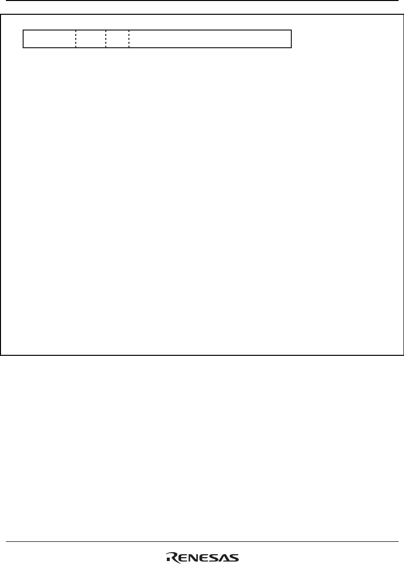
SR (Status register)
RB bit: Register bank bit; used to define the general registers.
RB = 1: R0_BANK1 to R7_BANK1 are used as general registers.
R0_BANK0 to R7_BANK0 accessed by LDC/STC instructions.
RB = 0: R0_BANK0 to R7_BANK0 are used as general registers.
R0_BANK1 to R7_BANK1 accessed by LDC/STC instructions.
BL bit: Block bit; used to mask exception.
BL = 1: Interrupts are masked (not accepted)
BL = 0: Interrupts are accepted
RC [11:0]: 12-bit repeat counter
DSP bit: DSP operation mode
DSP = 1: DSP instructions (LDS Rm, DSR/A0/X0/X1/Y0/Y1,
LDS.L @Rm+, DSR/A0/X0/X1/Y0/Y1, STS DSR/A0/X0/X1/Y0/Y1, Rn,
STS.L DSR/A0/X0/X1/Y0/Y1, @–Rn, LDC Rm, RS/RE/MOD,
LDC.L @Rm+, RS/RE/MOD, STC RS/RE/MOD,Rn, STC.L RS/RE/MOD, @–Rn,
LDRS, LDRE, SETRC, MOVS, MOVX, MOVY, Pxxx) are enabled.
DSP = 0: All DSP instructions are treated as illegal instructions; only SH3 instructions are
supported.
DMY bit: Modulo addressing enable for Y side
DMX bit: Modulo addressing enable for X side
Q, M bit: Used by DIV0U/S and DIV1 instructions.
I [3:0]: 4-bit field indicating the interrupt request mask level.
RF [1:0]: Used for repeat control
S bit: Used by the MAC instructions and DSP data.
T bit: The MOVT, CMP/cond, TAS, TST, BT, BF, SETT, CLRT and DT instructions use the T bit to indicate true
(logic one) or false (logic zero). The ADDV/C, SUBV/C, DIV0U/S, DIV1, NEGC, SHAR/L, SHLR/L,
ROTR/L and ROTCR/L instructions also use the T bit to indicate a carry, borrow, overflow, or underflow.
Reserved bits: A fixed value (either 0 or 1) is read from each of the bits. When writing, write the values shown in the
above register. Operation is not guaranteed if a value other than that given above is written to the
reserved bits.
Figure 2.5 Control Registers (1)


