


Section 12 Bus State Controller (BSC)
Rev. 4.00 Sep. 14, 2005 Page 273 of 982
REJ09B0023-0400
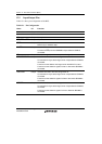
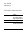
Name I/O Function
WE0 Output Indicates that D7 to D0 are being written to.
Connected to the byte select signal when a byte-selection SRAM is
connected.
Functions as the selection signals for D7 to D0 when SDRAM is
connected.
RASU
RASL
Output Connects to RAS pin when SDRAM is connected.
CASU
CASL
Output Connects to CAS pin when SDRAM is connected.
CKE Output Clock enable for SDRAM
FRAME Output Functions as FRAME signal when connected to burst MPX-IO
interface
WAIT Input External wait input
BREQ Input Bus request input
BACK Output Bus enable input
MD3 Input MD3: Select area 0 bus width (16/32 bits)
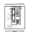
12.3 Area Overview
12.3.1 Area Division
In the architecture of this LSI, both logical spaces and physical spaces have 32-bit address spaces.
The cache access method is shown by the upper three bits. For details see section 7, Cache. The
remaining 29 bits are used for division of the space into ten areas (address map 1) or eight areas
(address map 2) according to the MAP bit in the CMNCR register setting. The BSC performs
control for this 29-bit space.
As listed in tables 12.2 and 12.3, this LSI can connect various memories to eight areas or six areas,
and it outputs chip select signals (CS0, CS2 to CS4, CS5A, CS5B, CS6A, and CS6B) for each of
them. CS0 is asserted during area 0 access; CS5A is asserted during area 5A access when address
map 1 is selected; and CS5B is asserted when address map 2 is selected. Also CS6A is asserted
during area 6A access when address map 1 is selected; and CS6B is asserted when address map 2
is selected.