


Section 12 Bus State Controller (BSC)
Rev. 4.00 Sep. 14, 2005 Page 321 of 982
REJ09B0023-0400
12.5 Operating Description
12.5.1 Endian/Access Size and Data Alignment
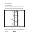
This LSI supports big endian, in which the 0 address is the most significant byte (MSByte) in the
byte data.
Three data bus widths (8 bits, 16 bits, and 32 bits) are available for normal memory and byte-
selection SRAM. Two data bus width (16 bits and 32 bits) are available for SDRAM. Data bus
width for MPX-IO is fixed to 32 bits. Data alignment is performed in accordance with the data bus
width of the device. This also means that when longword data is read from a byte-width device,
the read operation must be done four times. In this LSI, data alignment and conversion of data
length is performed automatically between the respective interfaces.
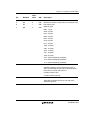
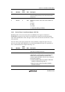
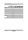
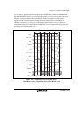
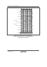
Table 12.5 through 12.7 show the relationship between device data width and access unit.
Table 12.5 32-Bit External Device Access and Data Alignment
Data Bus Strobe Signals
Operation
D31 to
D24
D23 to
D16
D15 to
D8 D7 to D0
WE3,
DQMUU
WE2,
DQMUL
WE1,
DQMLU
WE0,
DQMLL
Byte access
at 0
Data
7 to 0
Assert
Byte access
at 1
Data
7 to 0
Assert
Byte access
at 2
Data
7 to 0
Assert
Byte access
at 3
Data
7 to 0
Assert
Word access
at 0
Data
15 to 8
Data
7 to 0
Assert Assert
Word access
at 2
Data
15 to 8
Data
7 to 0
Assert Assert
Longword
access at 0
Data
31 to 24
Data
23 to 16
Data
15 to 8
Data
7 to 0
Assert Assert Assert Assert