


Section 12 Bus State Controller (BSC)
Rev. 4.00 Sep. 14, 2005 Page 388 of 982
REJ09B0023-0400
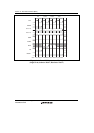
6. Data output from an external device caused by DMA single address transfer is followed by
data output from another device that includes this LSI (DMAIWA = 0)
For details, see the description of the DMAIWA bit in the CMNCR register.
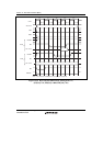
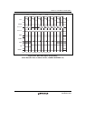
7. Data output from an external device caused by DMA single address transfer is followed by any
type of access (DMAIWA = 1)
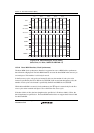
Besides the wait cycles between access cycles (idle cycles) described above, idle cycles must be
inserted to reserve the minimum pulse width for an interface with an internal bus and a
multiplexed pin (WEn).
8. Idle cycle of the external bus for the interface with the internal bus
A. Insert one idle cycle immediately before a write access cycle after an external bus idle
cycle or a read cycle.
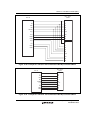
B. Insert one idle cycle to transfer the read data to the internal bus when a read cycle of the
external bus terminates.
Insert two to three idle cycles including the idle cycle in A. for the write cycle immediately
after a read cycle.
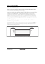
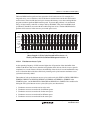
9. Idle cycle of the external bus for accessing different memory
For accessing different memory, insert idle cycles as follows. The byte-selection SRAM
interface with the BAS bit = 1 specified is handled as an SDRAM interface because the WEn
change timing is identical.
A. Insert one idle cycle to access the interface other than the SDRAM interface after the write
access cycle is performed in the SDRAM interface.
B. Insert one idle cycle to access the SDRAM interface after the normal space interface with
the external wait invalidated or the byte-selection SRAM interface with the BAS bit = 0
specified is accessed.
C. Insert one idle cycle to access the SDRAM interface after the MPX-IO interface is
accessed.
D. Insert one idle cycle to access the MPX-IO interface from the external bus that is in the idle
status.
E. Insert one idle cycle to access the MPX-IO interface after a read cycle is performed in the
normal space interface, byte-selection SRAM interface with the BAS bit = 0 specified or
the SDRAM interface.
F. Insert two idle cycles to access the MPX-IO interface after a write cycle is performed in the
SDRAM interface.
G. Insert one idle cycle to access the SDRAM interface which is not in the low frequency
mode after the interface in the SDRAM low frequency mode (SDCR.SLOW = 1) is
accessed.