Section 22 Pin Function Controller (PFC)
Rev. 4.00 Sep. 14, 2005 Page 842 of 982
REJ09B0023-0400
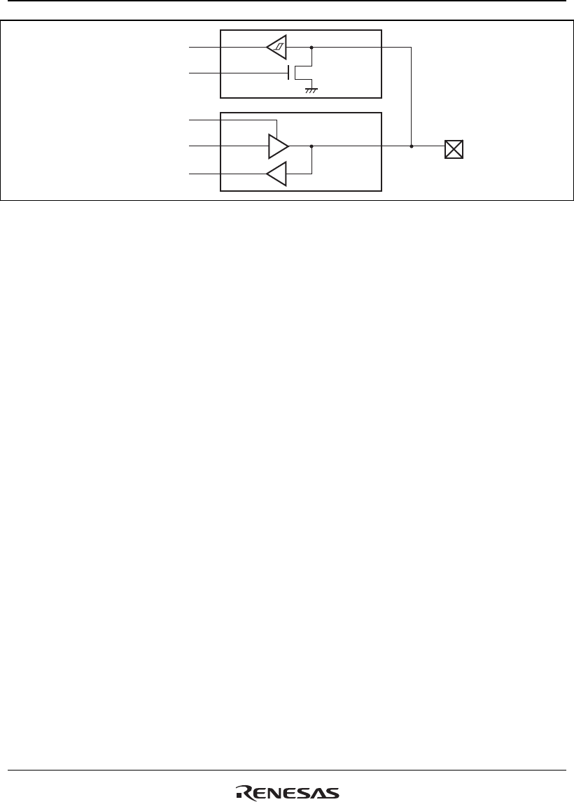
SDA input data
SCL input data
SDA output data
SCL output data
PTG[10] output enable
PTG[9] output enable
PTG[10] output data
PTG[9] output data
PTG[10] input data
PTG[9] input data
PTG[10] /SDA
PTG[9] /SCL
Figure 22.2 Internal Block Diagram of I/O Buffer with Open Drain
22.3 Notes on Usage
• Pins function as outputs when other function is selected by the port control register
When the pin function (shown in table 22.1, List of Multiplexed Pins) is changed from other
function (output) to port function (input), the weak keeper in figure 22.1 holds the value of the
port data register of the pin.
• Pins function as inputs/outputs when other function is selected by the port control register
When the pin function (shown in table 22.1, List of Multiplexed Pins) is changed from port
function (input) to other function (output), the weak keeper in figure 22.1 holds the other
function value of the pin.
• Pins PTG10 and PTG9
The I/O buffers of PG10 and PTG9 have no weak keeper. When you do not use these pins, pull
up or pull down them. If you use them as port input, do not apply mid-voltage.
• Pins with weak keepers
Immediately after a power-on reset, the level of the pin which has a weak keeper is not
undefined whether high or low. Thus, to fix the pin level, the pin needs to be pulled up or
down.
Reference pull-up and pull-down resistances are shown below. These resistances change
according to the circuit configuration.
Pull-up resistance (reference value) = 2 kΩ
Pull-down resistance (reference value) = 8 kΩ


