


Section 12 Bus State Controller (BSC)
Rev. 4.00 Sep. 14, 2005 Page 335 of 982
REJ09B0023-0400
12.5.6 SDRAM Interface
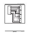
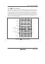
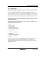
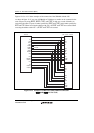
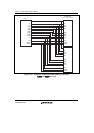
SDRAM Direct Connection: The SDRAM that can be connected to this LSI is a product that has
11/12/13 bits of row address, 8/9/10 bits of column address, 4 or less banks, and uses the A10 pin
for setting precharge mode in read and write command cycles. The control signals for direct
connection of SDRAM are RASU, RASL, CASU, CASL, RD/WR, DQMUU, DQMUL, DQMLU,
DQMLL, CKE, CS2, and CS3. All the signals other than CS2 and CS3 are common to all areas,
and signals other than CKE are valid when CS2 or CS3 is asserted. SDRAM can be connected to
up to 2 spaces. The data bus width of the area that is connected to SDRAM can be set to 32 or 16
bits.
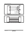
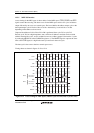
Burst read/single write (burst length 1) and burst read/burst write (burst length 1) are supported as
the SDRAM operating mode.
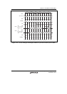
Commands for SDRAM can be specified by RASU, RASL, CASU, CASL, RD/WR, and specific
address signals. These commands supports:
• NOP
• Auto-refresh (REF)
• Self-refresh (SELF)
• All banks pre-charge (PALL)
• Specified bank pre-charge (PRE)
• Bank active (ACTV)
• Read (READ)
• Read with pre-charge (READA)
• Write (WRIT)
• Write with pre-charge (WRITA)
• Write mode register (MRS)
• EMRS
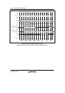
The byte to be accessed is specified by DQMUU, DQMUL, DQMLU, and DQMLL. Reading or
writing is performed for a byte whose corresponding DQMxx is low. For details on the
relationship between DQMxx and the byte to be accessed, refer to section 12.5.1, Endian/Access
Size and Data Alignment.