


997
Chapter 54 Flash Memory
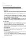
6.Flash Access Mode Switching
6. Flash Access Mode Switching
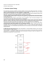
On MB91460 series flash devices it is possible to switch between different flash access modes. These modes are
depending on device type.
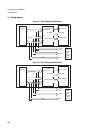
The 16bit mode is intended basically for flash programming, so program execution from flash is prohibited anyway.
The 32bit and 64bit modes, however, are intended for program execution from flash. Since switching between
these modes directly from an application located in the flash is prohibited it is necessary to locate the switching
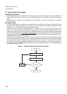
routine either in RAM or use the available routine in the Boot ROM:
This routine is located at address 0xBF60 for all MB91F46x devices. To call this function two parameters are
expected in CPU registers R4 and R5:
R4: 2bits (LSB of register) for setting the flash access mode
b’00: 32bit read/write mode
b’01: 16bit read/write mode
b’1x: 64bit read only mode
R5: 16bits for setting wait time
The wait time should be in the range of some 100ns after switching the flash access mode for stabilization of the
Flash-ROM. The wait function is a simple delay loop that needs about 3 CPU cycles for one run. The value in R5
represents the number of runs through this delay loop.
Example (time for 1 run through delay loop):
30 ns @ 100MHz CPU clock min. 4-5 runs
47 ns @ 64MHz CPU clock min. 3 runs
94 ns @ 32MHz CPU clock min. 2 runs
500 ns @ 2MHz CPU clock min. 1 runs
After leaving this delay loop, the switching function will return to the application.
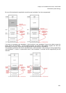
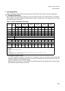
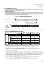
Device 16bit access 32bit access 64bit access
MB91F467DA read/write read/write read
MB91F469GA read/write read/write read
MB91F464AA read/write read -
MB91F465KA read/write read -