


507
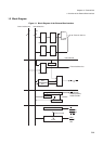
Chapter 31 External Bus
1.Overview of the External Bus Interface
Chapter 31 External Bus
The external bus interface controller controls the interfaces with the internal bus for chips and
with external memory and I/O devices.
This chapter explains each function of the external bus interface and its operation.
1. Overview of the External Bus Interface
1.1 Features
● The external bus interface has the following features:
• Addresses of up to 32 bits (4 GB space) can be output.
• Various kinds of external memory (8-bit/16-bit/32-bit modules) can be directly connected and multiple
access timings can be mixed and controlled.
• Asynchronous SRAM and asynchronous ROM/FLASH memory (multiple write strobe method or byte enable
method)
• Page mode ROM/FLASH memory (Page sizes 2, 4, and 8 can be used)
• Burst mode ROM/FLASH memory (such as MBM29BL160D/161D/162D)
• Address/data multiplex bus (8-bit/16-bit width only)
• SDRAM (FCRAM modules are also supported, including two - and four - bank types with CAS latency 1 to 8)
• Synchronous memory (such as ASIC built-in memory) (Synchronous SRAM cannot be directly connected)
• Eight independent banks (chip select areas) can be set, and chip select corresponding to each bank can be
output.
• The size of each area can be set in multiples of 64 KB (64 KB to 2 GB for each chip select area).
• An area can be set at any location in the logical address space (Boundaries may be limited depending on
the size of the area.)
● In each chip select area, the following functions can be set independently:
• Enabling and disabling of the chip select area (Disabled areas cannot be accessed)
• Setting of the access timing type to support various kinds of memory
• Detailed access timing setting (individual setting of the access type such as the wait cycle)
• Setting of the data bus width (8-bit/16-bit)
• Setting of the order of bytes (big or little endian) (Only big endian can be set for the CS0 area)
• Setting of write disable (read-only area)
• Enabling and disabling of fetches from the built-in cache
• Enabling and disabling of the prefetch function
• Maximum burst length setting (1, 2, 4, 8)
● A different detailed timing can be set for each access timing type.
• For the same type of access timing, a different setting can be made in each chip select area.
• Auto-wait can be set to up to 15 cycles (asynchronous SRAM, ROM, Flash, and I/O area).
• The bus cycle can be extended by external RDY input (asynchronous SRAM, ROM, Flash, and I/O area).
• The first access wait and page wait can be set (burst, page mode, and ROM/FLASH area).
• Various kinds of idle/recovery cycles and setting delays can be inserted.