


582
Chapter 31 External Bus
9.SDRAM/FCRAM Interface Operation
9. SDRAM/FCRAM Interface Operation
This section describes the operations of the SDRAM/FCRAM interface.
■ SDRAM/FCRAM interface
The chip select areas can be used as SDRAM/FCRAM interface by setting the TYP3 to TYP0 bits in the area
configuration register (ACR) to 100X
B
.
This section provides timing charts to describe the following operations of the SDRAM/FCRAM interface.
• Burst read/write (Settings: Page hit, CAS latency 2)
• Single read/write (Settings: Page hit, CAS latency 3, auto - precharge OFF)
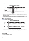
• Single read (Settings: Page miss, CAS latency 3, auto - precharge OFF)
• Single read/write (Settings: CAS latency 1, TYP 1001
B
, auto - precharge ON)
• Auto - refresh
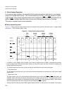
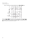
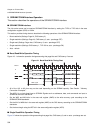
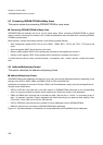
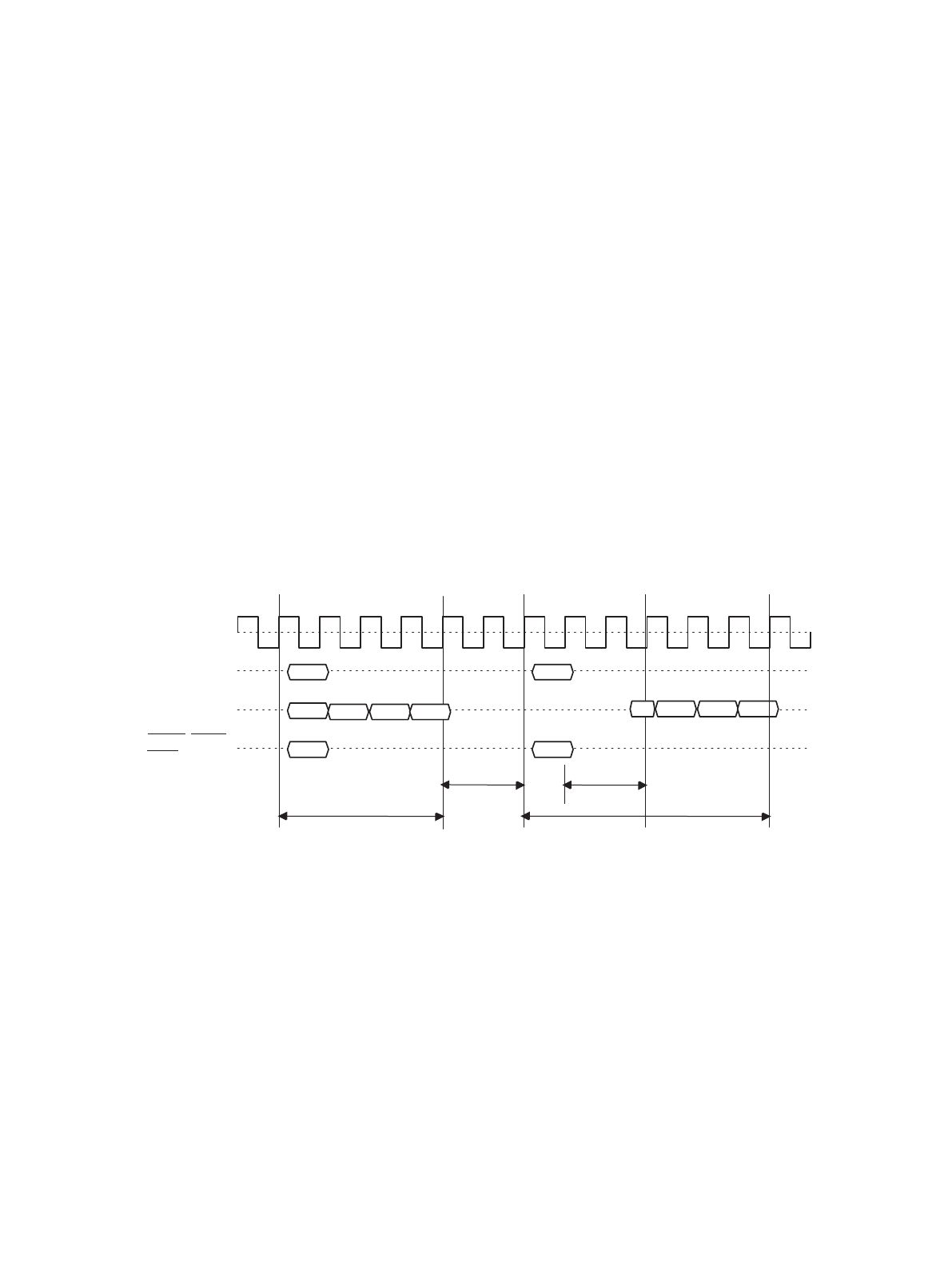
■ Burst Read/Write Operation Timing
Figure 4.9 - 1 shows the operation timings assuming that page hits and CAS latency 2 are set.
Figure 9-1 Burst Read/Write Timing Chart
• All of the A13 to A0 pins may not be used depending on the SDRAM capacity. See Section " Memory
Connection Examples " .
• The MCLK is a clock signal input to SDRAM. Signals such as addresses, data, and commands are input to
SDRAM at the rise of the MCLK.
• Set the W05 and W04 bits in the area wait register (AWR) to the write recovery cycle according to the
SDRAM/FCRAM standards.
• Set the W10 to W08 bits in the area wait register (AWR) to the CAS latency according to the SDRAM/FCRAM
standards.
• Set the burst length using the BST bit in the area configuration register (ACR).
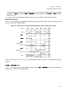
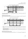
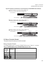
■ Single Read/Write Operation Timing
Figure 9-2 shows the operation timings assuming that page hits, CAS latency 3, and no auto - precharge are set.
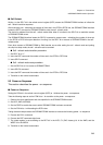
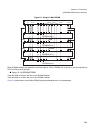
MCLK
A
SRAS,SCAS,
SWE
D
Read cycle
Cas Latency
#1
#1
READ
Write cycle
#1
#1
WRIT
Write recovery
#2 #3 #4
#2 #3 #4