


630
Chapter 32 USART (LIN / FIFO)
4.USART Registers
* see table 4-7 for SOPE and SIOP interaction
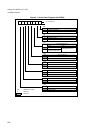
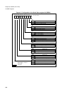
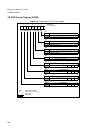
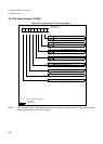
4.6 Extended Communication Control Register (ECCR04)
The extended communication control register provides bus idle recognition, interrupt settings, synchronous
clock settings, and the LIN break generation.
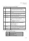
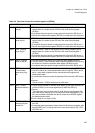
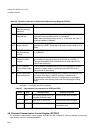
Table 4-6 Function of each bit of the Extended Status/Control Register (ESCR4)
Bit name Function
bit15 LBIE: LIN break
detection interrupt
enable bit
This bit enables a reception interrupt, if a LIN break was detected.
bit14 LBD: LIN break
detected flag
This bit goes 1 if a LIN break was detected. Writing a 0 to it clears this
bit and the corresponding interrupt, if it is enabled.
Note: RMW instructions always return "1". In this case, the value "1"
does not indicate a LIN-Break.
bit13
bit12
LBL1/0: LIN break
length selection
These two bits determine how many serial bit times the LIN break is
generated by USART. Receiving a LIN break is always fixed to 13 bit
times.
bit11 SOPE: Serial Output
pin direct access
enable*
Setting this bit to 1 enables the direct write to the SOT04 pin, if SOE
= 1 (SMR04).*
bit10 SIOP: Serial Input/
Output Pin direct
access*
Normal read instructions always return the actual value of the SIN04
pin. Writing to it sets the bit value to the SOT04 pin, if SOPE = 1.
During a Read-Modify-Write instruction the bit returns the SOT04
value in the read cycle.*
bit9 CCO: Continuos
Clock Output enable
bit
This bit enables a continuos serial clock at the SCK04 pin if USART
operates in master mode 2 (synchronous) and the SCK04 pin is
configured as a clock output.
bit8 SCES: Serial clock
edge selection bit
This bit inverts the internal serial clock in mode 2 (synchronous) and
the output clock signal, if USART operates in master mode 2
(synchronous) and the SCK04 pin is configured as a clock output.
In slave mode 2 the sampling time turns from rising edge to falling
edge.
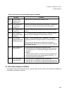
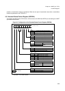
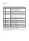
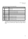
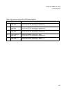
Table 4-7 * Description of the interaction of SOPE and SIOP:
SOPE SIOP Writing to SIOP Reading from SIOP
0 R/W has no effect on the SOT4 pin
but holds the written value.
returns current value of SIN04
1 R/W write "0" or "1" to SOT04 returns current value of SIN04
1 RMW returns current value of SOT04
and writes it back