


536
Chapter 31 External Bus
2.External Bus Interface Registers
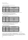
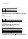
[Bits 23-16] CHE7-0 (Cache Enable 7-0)
These bits enable and disable each chip select area for transfers to the built-in cache.
2.9 Pin/Timing Control Register (TCR)
This section explains the configuration and functions of the pin/timing control register and its
function.
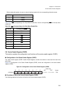
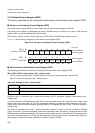
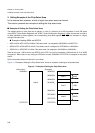
■ Configuration of the Pin/Timing Control Register (TCR)
The pin/timing control register (TCR: Terminal and Limiting Control Register) controls the functions related to the
general external bus interface controller, such as the setting of common pin functions and timing control.
Figure 2-9 "Configuration of the Pin/Timing Control Register (TCR)" shows the configuration of the pin/timing
control register (TCR).
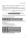
Figure 2-9 Configuration of the Pin/Timing Control Register (TCR)
■ Functions of Bits in the Pin/Timing Control Register (TCR)
The following explains the functions of the bits in the pin/timing control register (TCR).
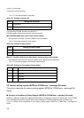
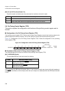
[Bit 7] BREN (BRQ Enable)
This bit enables BRQ pin input and external bus sharing.
In the initial state (0), BRQ input is ignored. When 1 is set, the bus is made open (control with high impedance)
and BGRNT is activated (L level is output) when the bus is ready to be made open after the BRQ input becomes
H level.
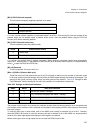
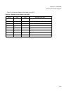
CHEn Cache area setting
0 Not a cache area (data read from the applicable area is not saved in the cache)
1 Cache area (data read from the applicable area is saved in the cache)
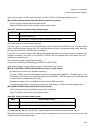
BREN BRQ input enable setting
0
No bus sharing by BRQ/BGRNT.
BRQ input is disabled.
1
Bus sharing by BRQ/BGRNT.
BRQ input is enabled.
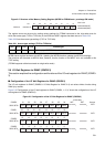
7 6 5 4 3 2 1 0
00000683
H
BREN PSUS PCLR
Reserved
Reserved
Reserved
RDW1 RDW0 00000000
B
0000xxxx
B
R/W
Initial value
INIT RST Access